7 parallel programming, 1 enter programming mode, Table 31-12 on – Rainbow Electronics ATmega128RFA1 User Manual
Page 469: Table 31-13 on, Atmega128rfa1
469
8266A-MCU Wireless-12/09
ATmega128RFA1
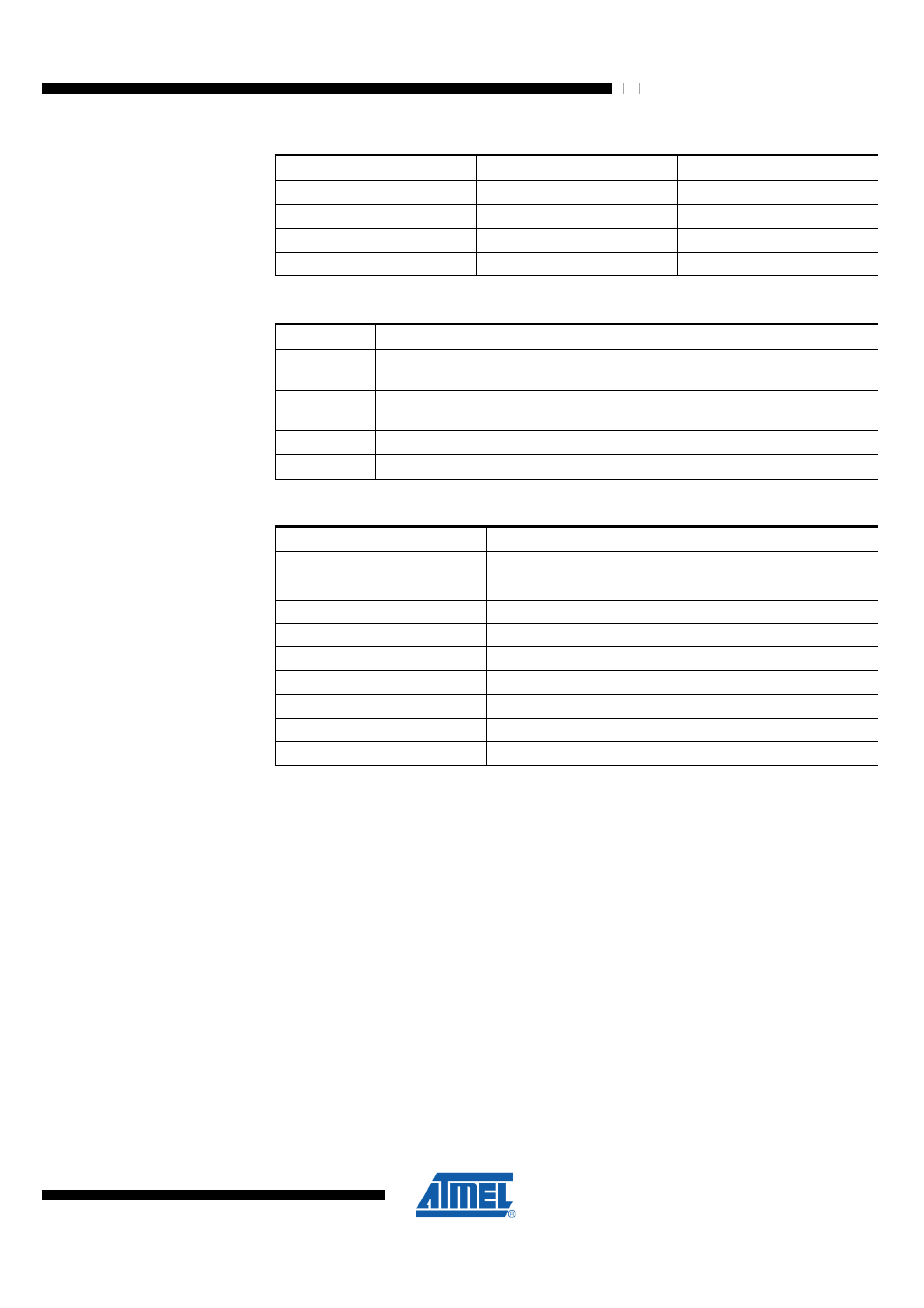
Table 31-11. Pin Values Used to Enter Programming Mode
Pin
Symbol
Value
PAGEL
Prog_enable[3]
0
XA1
Prog_enable[2]
0
XA0
Prog_enable[1]
0
BS1
Prog_enable[0]
0
Table 31-12. XA1 and XA0 Encoding
XA1
XA0
Action when CLKI is Pulsed
0
0
Load Flash or EEPROM Address (High or low address byte
determined by BS2 and BS1).
0
1
Load Data (High or Low data byte for Flash determined by
BS1).
1
0
Load Command.
1
1
No Action, Idle.
Table 31-13. Command Byte Bit Encoding
Command Byte
Command Executed
1000 0000
Chip Erase
0100 0000
Write Fuse bits
0010 0000
Write Lock bits
0001 0000
Write Flash
0001 0001
Write EEPROM
0000 1000
Read Signature bytes and Calibration byte
0000 0100
Read Fuse and Lock bits
0000 0010
Read Flash
0000 0011
Read EEPROM
31.7 Parallel Programming
Pulses of CLKI and in the following command sequences are assumed to be at least
250 ns wide unless otherwise noted.
31.7.1 Enter Programming Mode
The following algorithm puts the device in parallel programming mode:
1. Apply 3.3V between DEVDD and DVSS.
2. Set RSTN to 0 and TST to 0.
3. Set the Prog_enable pins listed in
to “0000” and wait at least
100ns.
4. Set TST to 1. TST can be set high any time before but not after the rising edge of
RSTN (t
TSTRNH
).
5. Set RSTN to 1. Any activity on Prog_enable pins within 100 ns after RSTN is set to 1
will cause the device to fail entering programming mode.
6. Wait at least 50 µs before sending a command.