3 serial programming instruction set, Table 31-17, Atmega128rfa1 – Rainbow Electronics ATmega128RFA1 User Manual
Page 479
479
8266A-MCU Wireless-12/09
ATmega128RFA1
not, all four bytes of the instruction must be transmitted. If the 0x53 did not echo
back, give RSTN a positive pulse and issue a new Programming Enable command.
4. The Flash is programmed one page at a time. The memory page is loaded one byte
at a time by supplying the 7 LSB of the address and data together with the Load
Program Memory Page instruction. To ensure correct loading of the page, the data
low byte must be loaded before data high byte is applied for a given address. The
Program Memory Page is stored by loading the Write Program Memory Page
instruction with the address lines 15:8. If polling (RDY/BSY
¯ ¯ ¯ ) is not used, the user
must wait at least t
WD_FLASH
before issuing the next page (see
).
Accessing the serial programming interface before the Flash write operation
completes can result in incorrect programming.
5. The EEPROM array is programmed one byte at a time by supplying the address and
data together with the appropriate Write instruction. An EEPROM memory location is
first automatically erased before new data is written. If polling is not used, the user
must wait at least t
WD_EEPROM
before issuing the next byte (see
).
In a chip erased device, no 0xFFs in the data file(s) need to be programmed.
6. Any memory location can be verified by using the Read instruction which returns the
content at the selected address at serial output PDO.
7. At the end of the programming session, RSTN can be set high to commence normal
operation.
8. Power-off sequence (if needed): Set RESET to “1”. Turn DEVDD power off.
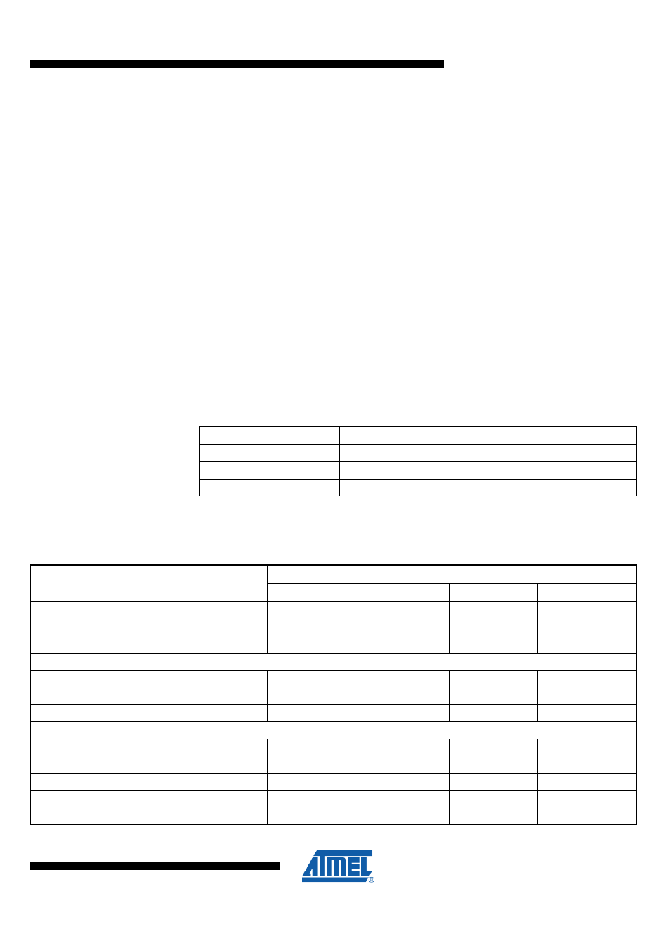
Table 31-16. Minimum Wait Delay before Writing the Next Flash or EEPROM Location
Symbol
Minimum Wait Delay
t
WD_FLASH
4.5 ms
t
WD_EEPROM
9 ms
t
WD_CHIPERASE
14.5 ms
31.8.3 Serial Programming Instruction Set
and
page 480 describe the Instruction set.
Table 31-17. Serial Programming Instruction Set
(4)(5)
Instruction Format
(1)
Instruction/Operation
Byte1
Byte2
Byte3
Byte4
Programming Enable
$AC
$53
$00
$00
Chip Erase (Program Memory/EEPROM)
$AC
$80
$00
$00
Poll RDY/BSY
¯ ¯ ¯
$F0
$00
$00
data byte out
Load Instruction
Load Program Memory Page, High Byte
$48
$00
addr. LSB
high data byte in
Load Program Memory Page, Low Byte
$40
$00
addr. LSB
low data byte in
Load EEPROM Memory Page (page access)
$C1
$00
0000 000aa
data byte in
Read Instruction
Read Program Memory, High byte
$28
addr. MSB
addr. LSB
high data byte out
Read Program Memory, Low byte
$20
addr. MSB
addr. LSB
low data byte out
Read EEPROM Memory
$A0
0000 aaaa
aaaa aaaa
data byte out
Read Lock Bits
$58
$00
$00
data byte out
Read Signature Byte
$30
$00
0000 000aa
data byte out