3 data mode, Atmega128rfa1 – Rainbow Electronics ATmega128RFA1 User Manual
Page 335
335
8266A-MCU Wireless-12/09
ATmega128RFA1
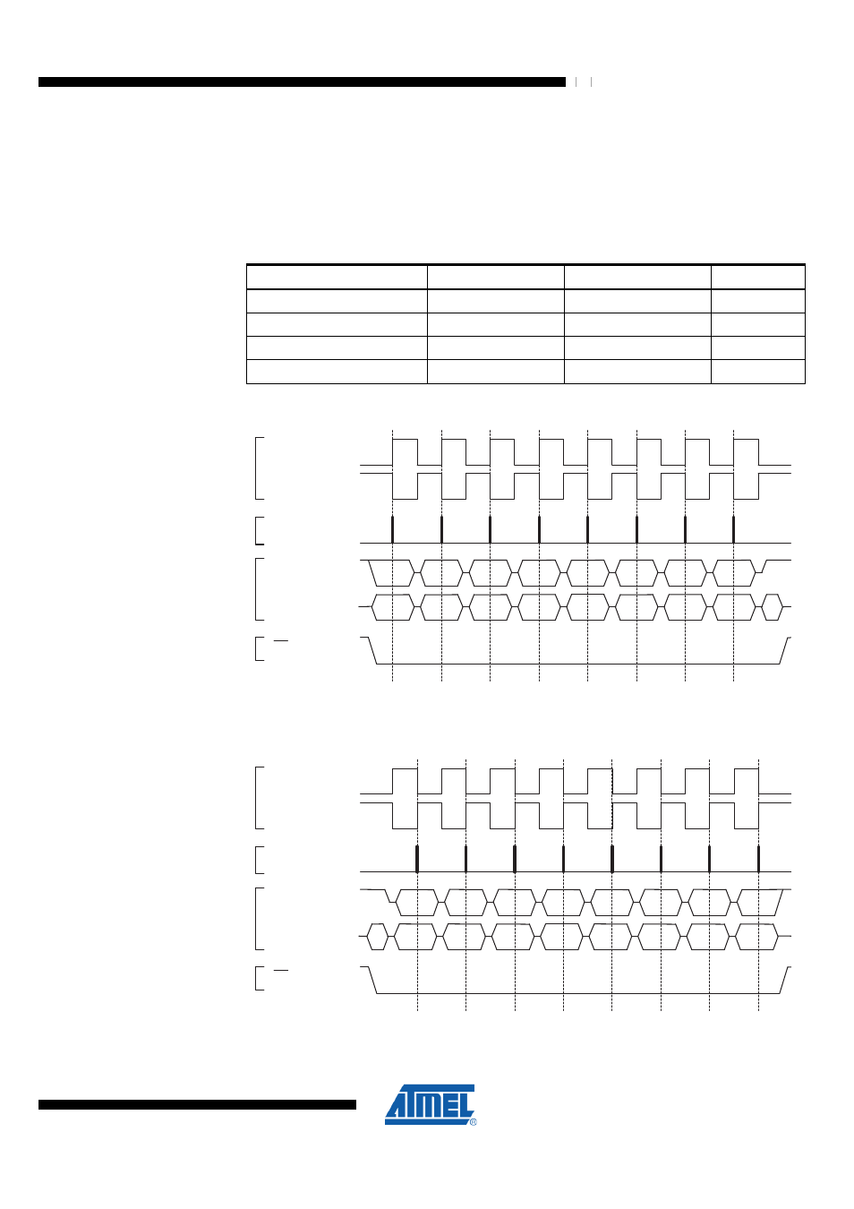
22.3.3 Data Mode
There are four combinations of SCK phase and polarity with respect to serial data,
which are determined by control bits CPHA and CPOL. The SPI data transfer formats
are shown in
. Data bits are shifted out and
latched in on opposite edges of the SCK signal, ensuring sufficient time for data signals
to stabilize. This is clearly seen in the summary of
:
Table 22-2. CPOL Functionality
Leading Edge
Trailing Edge
SPI Mode
CPOL=0, CPHA=0
Sample (Rising)
Setup (Falling)
0
CPOL=0, CPHA=1
Setup (Rising)
Sample (Falling)
1
CPOL=1, CPHA=0
Sample (Falling)
Setup (Rising)
2
CPOL=1, CPHA=1
Setup (Falling)
Sample (Rising)
3
Figure 22-3. SPI Transfer Format with CPHA = 0
Bit 1
Bit 6
LSB
MSB
SCK (CPOL = 0)
mode 0
SAMPLE I
MOSI/MISO
CHANGE 0
MOSI PIN
CHANGE 0
MISO PIN
SCK (CPOL = 1)
mode 2
SS
MSB
LSB
Bit 6
Bit 1
Bit 5
Bit 2
Bit 4
Bit 3
Bit 3
Bit 4
Bit 2
Bit 5
MSB first (DORD = 0)
LSB first (DORD = 1)
Figure 22-4. SPI Transfer Format with CPHA = 1
SCK (CPOL = 0)
mode 1
SAMPLE I
MOSI/MISO
CHANGE 0
MOSI PIN
CHANGE 0
MISO PIN
SCK (CPOL = 1)
mode 3
SS
MSB
LSB
Bit 6
Bit 1
Bit 5
Bit 2
Bit 4
Bit 3
Bit 3
Bit 4
Bit 2
Bit 5
Bit 1
Bit 6
LSB
MSB
MSB first (DORD = 0)
LSB first (DORD = 1)