5 adcl and adch - the adc data register, 1 adlar = 0, 2 adlar = 1 – Rainbow Electronics ATmega128RFA1 User Manual
Page 432: Atmega128rfa1
432
8266A-MCU Wireless-12/09
ATmega128RFA1
This register defines the track-and-hold time for sampling the analog input voltage of
the ADC and it defines the start-up time for the analog blocks based on a number of
ADC clock cycles. The ADC clock is generated from the system clock with the ADC
prescaler. The bits ADPS2:0 of register ADCSRA set the prescaler ratio. Correct start-
up and track-and-hold times are important for precise conversion results.
•
Bits 7:6 – ADTHT1:0: ADC Track-and-Hold Time
These bits define the number of ADC clock cycles for the sampling time of the analog
input voltage. For a complete description of this bit, see
•
Bit 5 – Res0: Reserved
•
Bits 4:0 – ADSUT4:0: ADC Start-up Time
These bits define the number of ADC clock cycles for the start-up time of the analog
blocks. For a complete description of this bit, see
"Pre-scaling and Conversion Timing"
.
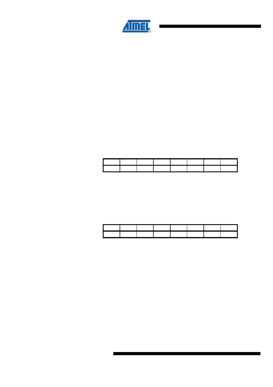
27.11.5 ADCL and ADCH – The ADC Data Register
27.11.5.1 ADLAR = 0
Bit
15
14
13
12
11
10
9
8
NA ($79)
–
–
–
–
–
–
ADC9
ADC8
ADCH
NA ($78)
ADC7
ADC6
ADC5
ADC4
ADC3
ADC2
ADC1
ADC0
ADCL
7
6
5
4
3
2
1
0
Read/Write
R
R
R
R
R
R
R
R
R
R
R
R
R
R
R
R
Initial Value
0
0
0
0
0
0
0
0
0
0
0
0
0
0
0
0
27.11.5.2 ADLAR = 1
Bit
15
14
13
12
11
10
9
8
NA ($79)
ADC9
ADC8
ADC7
ADC6
ADC5
ADC4
ADC3
ADC2
ADCH
NA ($78)
ADC1
ADC0
–
–
–
–
–
–
ADCL
7
6
5
4
3
2
1
0
Read/Write
R
R
R
R
R
R
R
R
R
R
R
R
R
R
R
R
Initial Value
0
0
0
0
0
0
0
0
0
0
0
0
0
0
0
0
When an A/D conversion is complete, the result is found in these two registers. If
differential channels are used, the result is presented in two’s complement form.
When ADCL is read, the ADC Data Register is not updated until ADCH is read.
Consequently, if the result is left adjusted and no more than 8-bit precision (7 bit + sign
bit for differential input channels) is required, it is sufficient to read ADCH. Otherwise,
ADCL must be read first, then ADCH.
The ADLAR bit in ADMUX, and the MUXn bits in ADMUX affect the way the result is
read from the registers. If ADLAR is set, the result is left adjusted. If ADLAR is cleared
(default), the result is right adjusted.