6 spi timing characteristics, Spi timing characteristics, Atmega128rfa1 – Rainbow Electronics ATmega128RFA1 User Manual
Page 504
504
8266A-MCU Wireless-12/09
ATmega128RFA1
Symbol
Parameter
Condition
Min.
Max.
Units
V
IH
Input High-voltage
0.7V
DEVDD
V
DEVDD
+0.5
V
V
hys
Hysteresis of Schmitt Trigger Inputs
V
V
OL
Output Low-voltage
3mA sink current
0
0.4
V
t
r
Rise Time for both SDA and SCL
300
ns
t
of
Output Fall Time from V
IHmin
to V
ILmax
250
ns
t
SP
Spikes suppressed by the input filter
50
ns
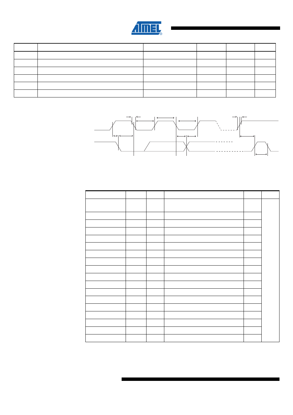
Figure 34-2
t
SU;STA
t
LOW
t
HIGH
t
LOW
t
of
t
HD;STA
t
HD;DAT
t
SU;DAT
t
SU;STO
t
BUF
SCL
SDA
t
r
34.6 SPI Timing Characteristics
See Figure 34-3and Figure 34-4 for details.
Table 34-9. SPI Timing Parameters
Description
Mode
Min
Typ
Max
Units
SCK period
Master
"SPCR – SPI Control Register" on
.
SCK high/low
Master
50% duty cycle
Rise/fall time
Master
TBD
Setup
Master
TBD
Hold
Master
TBD
Out to SCK
Master
0.5 t
SCK
SCK to out
Master
TBD
SCK to out high
Master
TBD
SS
__
low to out
Slave
TBD
SCK period
Slave
4 t
CK
SCK high/low
(
1
)
Slave
2 t
CK
Rise/fall time
Slave
TBD
Setup
Slave
TBD
Hold
Slave
t
CK
SCK to out
Slave
TBD
SCK to SS
__
high
Slave
TBD
SS
__
high to tri-state
Slave
TBD
SS
__
low to SCK
Slave
TBD
ns
Note:
1. In SPI Programming mode the minimum SCK high/low period is 2 t
CLCL
for f
CK
< 12
MHz and 3 t
CLCL
for f
CK
> 12 MHz.