17 tccr3b - timer/counter3 control register b, Atmega128rfa1 – Rainbow Electronics ATmega128RFA1 User Manual
Page 278
278
8266A-MCU Wireless-12/09
ATmega128RFA1
Register Bits
Value
Description
0xE
Fast PWM, TOP = ICRn
0xF
Fast PWM, TOP = OCRnA
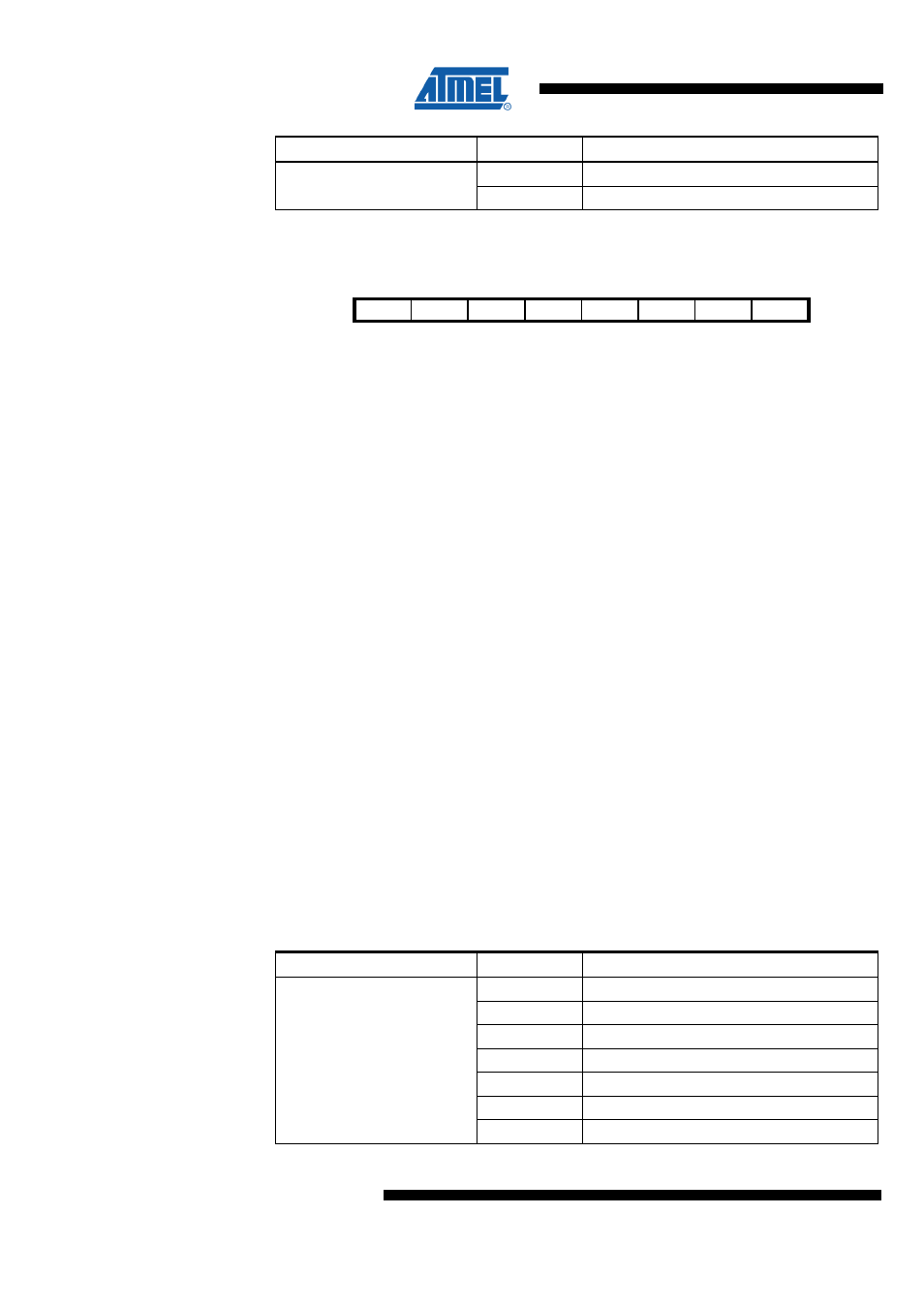
18.11.17 TCCR3B – Timer/Counter3 Control Register B
Bit
7
6
5
4
3
2
1
0
NA ($91)
ICNC3
ICES3
Res
WGM33 WGM32
CS32
CS31
CS30
TCCR3B
Read/Write
RW
RW
R
RW
RW
RW
RW
RW
Initial Value
0
0
0
0
0
0
0
0
•
Bit 7 – ICNC3 - Input Capture 3 Noise Canceller
Setting this bit (to one) activates the Input Capture Noise Canceler. When the Noise
Canceler is activated, the input from the Input Capture Pin (ICP3) is filtered. The filter
function requires four successive equal valued samples of the ICP3 pin for changing its
output. The input capture is therefore delayed by four Oscillator cycles when the noise
canceler is enabled.
•
Bit 6 – ICES3 - Input Capture 3 Edge Select
This bit selects which edge on the Input Capture Pin (ICP3) that is used to trigger a
capture event. When the ICES3 bit is written to zero, a falling (negative) edge is used
as trigger. When the ICES3 bit is written to one, a rising (positive) edge will trigger the
capture. When a capture is triggered according to the ICES3 setting, the counter value
is copied into the Input Capture Register (ICR3). The event will also set the Input
Capture Flag (ICF3). This can be used to cause an Input Capture Interrupt, if this
interrupt is enabled. When the ICR3 is used as TOP value (see description of the
WGM33:0 bits located in the TCCR3A and the TCCR3B Register), the ICP3 is
disconnected and consequently the input capture function is disabled.
•
Bit 5 – Res - Reserved Bit
This bit is reserved for future use. A read access always will return zero. A write access
does not modify the content.
•
Bit 4:3 – WGM31:30 - Waveform Generation Mode
Combined with the WGM31:0 bits found in the TCCR3A Register, these bits control the
counting sequence of the counter, the source for maximum (TOP) counter value, and
what type of waveform generation to be used. Modes of operation supported by the
Timer/Counter unit are: Normal mode (counter), Clear Timer on Compare match (CTC)
mode, and three types of Pulse Width Modulation (PWM) modes. For more information
on the different modes see section "Modes of Operation".
Table 18-16 WGM3 Register Bits
Register Bits
Value
Description
0x0
Normal mode of operation
0x1
PWM, phase correct, 8-bit
0x2
PWM, phase correct, 9-bit
0x3
PWM, phase correct, 10-bit
0x4
CTC, TOP = OCRnA
0x5
Fast PWM, 8-bit
WGM31:30
0x6
Fast PWM, 9-bit