11 register description, 1 timsk2 - timer/counter interrupt mask register, Register description" on – Rainbow Electronics ATmega128RFA1 User Manual
Page 323: Atmega128rfa1

323
8266A-MCU Wireless-12/09
ATmega128RFA1
The TOSC1 pin is selected by setting the EXCLKAMR bit in the ASSR register to logic
zero. Under this condition TOSC1 and TOSC2 are disconnected from Port G and a
crystal can then be connected between the TOSC1 and TOSC2 pins to serve as an
independent clock source for Timer/Counter2. The Oscillator is optimized for use with a
32.768 kHz crystal. By setting the EXCLK bit in the ASSR, a 32 kHz external clock can
be applied on TOSC1.
Setting the EXCLKAMR bit to logic one selects the AMR pin as the Timer/Counter2
clock source. Thus the 32 kHz oscillator can be used by the MAC symbol counter while
the Timer/Counter2 uses pin AMR as clock source, see
.
A complete overview of the implemented asynchronous clock sources can be found in
. The last column mentions which pins are available for GPIO
functionality. For details about the ASSR register refer to section
.
For Timer/Counter2, the possible pre-scaled selections are: clk
T2S
/8, clk
T2S
/32, clk
T2S
/64, clk
T2S
/128, clk
T2S
/256, and clk
T2S
/1024. Additionally, clk
T2S
as well as 0 (stop) may
be selected. Setting the PSRASY bit in GTCCR resets the prescaler. This allows the
user to operate with a predictable prescaler.
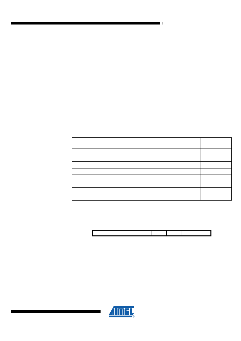
Table 21-6. Asynchronous clock selection for Timer/Counter2 and Symbol-Counter
AS2
EXCLK EXCLKAMR
Timer/Counter2
clock source
32 kHz crystal Osc.
(TOSC1/TOSC2)
PG2, PG3, PG4
as GPIOs
0
0
0
cp2io
off
PG2, PG3, PG4
0
1
0
not defined
not defined
not defined
1
0
0
32 kHz crystal Osc
on
PG2
1
1
0
TOSC1 (PG4)
off
PG2, PG3
0
0
1
cp2io
off
PG2, PG3, PG4
0
1
1
not defined
not defined
not defined
1
0
1
AMR (PG2)
on
1
1
1
AMR (PG2)
off
PG3, PG4
21.11 Register Description
21.11.1 TIMSK2 – Timer/Counter Interrupt Mask register
Bit
7
6
5
4
3
2
1
0
NA ($70)
Res4
Res3
Res2
Res1
Res0
OCIE2B OCIE2A
TOIE2
TIMSK2
Read/Write
R
R
R
R
R
RW
RW
RW
Initial Value
0
0
0
0
0
0
0
0
•
Bit 7:3 – Res4:0 - Reserved Bit
This bit is reserved for future use. A read access always will return zero. A write access
does not modify the content.
•
Bit 2 – OCIE2B - Timer/Counter2 Output Compare Match B Interrupt Enable
When the OCIE2B bit is written to one and the I-bit in the Status Register is set (one),
the Timer/Counter2 Compare Match B interrupt is enabled. The corresponding interrupt
is executed if a compare match in Timer/Counter2 occurs, i.e., when the OCF2B bit is
set in the Timer/Counter2 Interrupt Flag Register TIFR2.
