3 tccr0b - timer/counter0 control register b, Atmega128rfa1 – Rainbow Electronics ATmega128RFA1 User Manual
Page 240
240
8266A-MCU Wireless-12/09
ATmega128RFA1
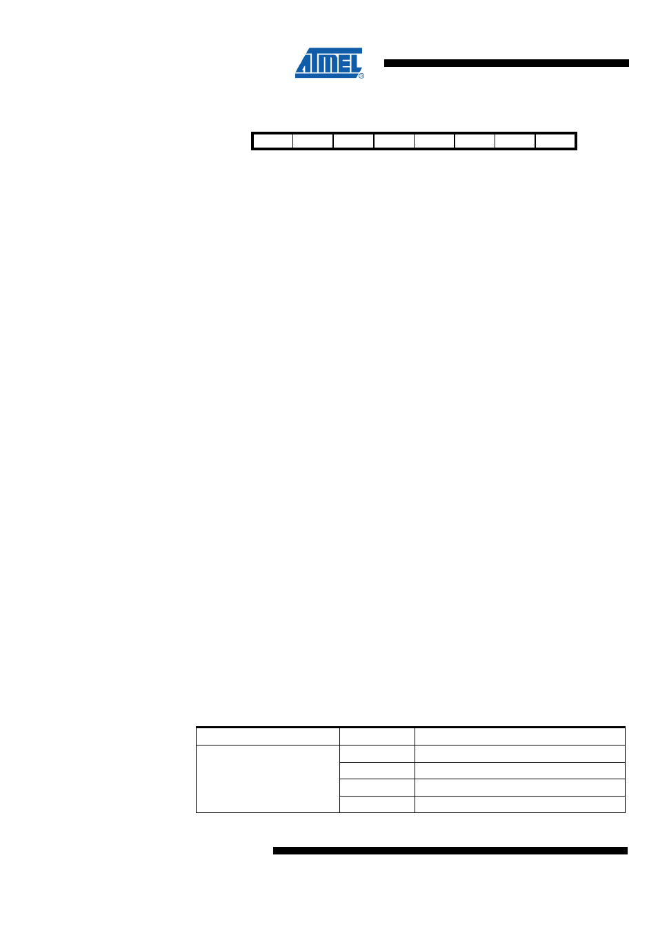
17.9.3 TCCR0B – Timer/Counter0 Control Register B
Bit
7
6
5
4
3
2
1
0
$25 ($45)
FOC0A
FOC0B
Res1
Res0
WGM02
CS02
CS01
CS00
TCCR0B
Read/Write
W
W
R
R
RW
RW
RW
RW
Initial Value
0
0
0
0
0
0
0
0
•
Bit 7 – FOC0A - Force Output Compare A
The FOC0A bit is only active when the WGM02:0 bits specify a non-PWM mode.
However, for ensuring compatibility with future devices, this bit must be set to zero
when TCCR0B is written in a PWM operation mode. When writing a logical one to the
FOC0A bit, an immediate Compare Match is forced on the Waveform Generation unit.
The OC0A output is changed according to its COM0A1:0 bits setting. Note that the
FOC0A bit is implemented as a strobe. Therefore it is the value present in the
COM0A1:0 bits that determines the effect of the forced compare. A FOC0A strobe will
not generate any interrupt nor will it clear the timer in CTC mode using OCR0A as TOP.
The FOC0A bit is always read as zero.
•
Bit 6 – FOC0B - Force Output Compare B
The FOC0B bit is only active when the WGM02:0 bits specify a non-PWM mode.
However, for ensuring compatibility with future devices, this bit must be set to zero
when TCCR0B is written in a PWM operation mode. When writing a logical one to the
FOC0B bit, an immediate Compare Match is forced on the Waveform Generation unit.
The OC0B output is changed according to its COM0B1:0 bits setting. Note that the
FOC0B bit is implemented as a strobe. Therefore it is the value present in the
COM0B1:0 bits that determines the effect of the forced compare. A FOC0B strobe will
not generate any interrupt nor will it clear the timer in CTC mode using OCR0B as TOP.
The FOC0B bit is always read as zero.
•
Bit 5:4 – Res1:0 - Reserved Bit
This bit is reserved for future use. A read access always will return zero. A write access
does not modify the content.
•
Bit 3 – WGM02 -
Combined with the WGM01:0 bit found in the TCCR0A Register, these bits control the
counting sequence of the counter, the source for maximum (TOP) counter value, and
what type of waveform generation to be used. Modes of operation supported by the
Timer/Counter unit are: Normal mode (counter), Clear Timer on Compare Match (CTC)
mode, and two types of Pulse Width Modulation (PWM) modes (see section "Modes of
Operation").
•
Bit 2:0 – CS02:00 - Clock Select
The three Clock Select bits select the clock source to be used by the Timer/Counter0
according to the following table.If external pin modes are used for Timer/Counter0,
transitions on the T0 pin will clock the counter even if the pin is configured as an output.
This feature allows software control of the counting.
Table 17-9 CS0 Register Bits
Register Bits
Value
Description
0x00
No clock source (Timer/Counter0 stopped)
0x01
clk_IO/1 (no prescaling)
0x02
clk_IO/8 (from prescaler)
CS02:00
0x03
clk_IO/64 (from prescaler)