11 register description, 1 tccr1a - timer/counter1 control register a, Register description" on – Rainbow Electronics ATmega128RFA1 User Manual
Page 266: Atmega128rfa1
266
8266A-MCU Wireless-12/09
ATmega128RFA1
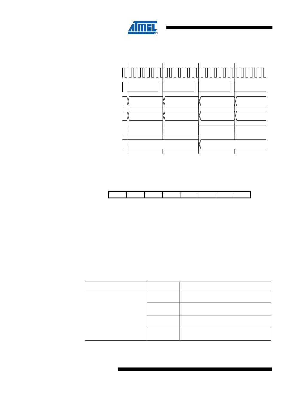
Figure 18-13 shows the same timing data, but with the prescaler enabled.
Figure 18-13. Timer/Counter Timing Diagram with Prescaler (f
clk_I/O
/8)
TOVn
(FPWM)
and ICF n
(if used
as TOP)
OCRnx
(Update at TOP)
TCNTn
(CTC and FPWM)
TCNTn
(PC and PFC PWM)
TOP - 1
TOP
TOP - 1
TOP - 2
Old OCRnx Value
New OCRnx Value
TOP - 1
TOP
BOTTOM
BOTTOM + 1
clk
I/O
clk
Tn
(clk
I/O
/8)
18.11 Register Description
18.11.1 TCCR1A – Timer/Counter1 Control Register A
Bit
7
6
5
4
3
2
1
0
NA ($80)
COM1A1 COM1A0 COM1B1 COM1B0 COM1C1 COM1C0 WGM11 WGM10
TCCR1A
Read/Write
RW
RW
RW
RW
RW
RW
RW
RW
Initial Value
0
0
0
0
0
0
0
0
•
Bit 7:6 – COM1A1:0 - Compare Output Mode for Channel A
The COM1A1:0 bits control the output compare behavior of pin OC1A. If one or both of
the COM1A1:0 bits are written to one, the OC1A output overrides the normal port
functionality of the I/O pin it is connected to. However note that the Data Direction
Register (DDR) bit corresponding to the OC1A pin must be set in order to enable the
output driver. When the OC1A is connected to the pin, the function of the COM1A1:0
bits is dependent of the WGM13:0 bits setting. The following table shows the
COM1A1:0 bit functionality when the WGM13:0 bits are set to a normal or a CTC mode
(non-PWM). For the other functionality refer to section "Modes of Operation".
Table 18-6 COM1A Register Bits
Register Bits
Value
Description
0
Normal port operation, OCnA/OCnB/OCnC
disconnected.
1
Toggle OCnA/OCnB/OCnC on Compare
Match.
2
Clear OCnA/OCnB/OCnC on Compare
Match (set output to low level).
COM1A1:0
3
Set OCnA/OCnB/OCnC on Compare Match
(set output to high level).
•
Bit 5:4 – COM1B1:0 - Compare Output Mode for Channel B