2 adcsrb - adc control and status register b, 3 didr1 - digital input disable register 1, Didr1 – digital input disable register 1" on – Rainbow Electronics ATmega128RFA1 User Manual
Page 409: Atmega128rfa1
409
8266A-MCU Wireless-12/09
ATmega128RFA1
•
Bit 1:0 – ACIS1:0 - Analog Comparator Interrupt Mode Select
These bits determine which comparator events that trigger the Analog Comparator
interrupt. The different settings are shown in the following table. When changing the
ACIS1/ACIS0 bits, the Analog Comparator Interrupt must be disabled by clearing its
Interrupt Enable bit in the ACSR Register. Otherwise an interrupt can occur when the
bits are changed.
Table 26-2 ACIS Register Bits
Register Bits
Value
Description
0x00
Interrupt on Toggle
0x01
Reserved
0x02
Interrupt on Falling Edge
ACIS1:0
0x03
Interrupt on Rising Edge
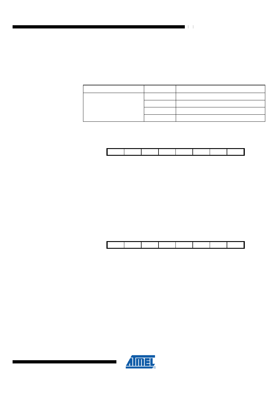
26.2.2 ADCSRB – ADC Control and Status Register B
Bit
7
6
5
4
3
2
1
0
NA ($7B)
ACME
ADCSRB
Read/Write
RW
Initial Value
0
•
Bit 6 – ACME - Analog Comparator Multiplexer Enable
When this bit is written logic one and the ADC is switched off (ADEN in ADCSRA is
zero), the ADC multiplexer defines the negative input of the Analog Comparator. When
this bit is written logic zero, AIN1 is applied to the negative input of the Analog
Comparator. For a detailed description of this bit, see section "Analog Comparator
Multiplexed Input".
26.2.3 DIDR1 – Digital Input Disable Register 1
Bit
7
6
5
4
3
2
1
0
NA ($7F)
AIN1D
AIN0D
DIDR1
Read/Write
RW
RW
Initial Value
0
0
•
Bit 1 – AIN1D - AIN1 Digital Input Disable
When this bit is written logic one, the digital input buffer on the AIN1 pin is disabled. The
corresponding PIN Register bit will always read as zero when this bit is set. When an
analog signal is applied to the AIN1 pin and the digital input from this pin is not needed,
this bit should be written logic one to reduce power consumption in the digital input
buffer.
•
Bit 0 – AIN0D - AIN0 Digital Input Disable
When this bit is written logic one, the digital input buffer on the AIN0 pin is disabled. The
corresponding PIN Register bit will always read as zero when this bit is set. When an
analog signal is applied to the AIN0 pin and the digital input from this pin is not needed,
this bit should be written logic one to reduce power consumption in the digital input
buffer.