6 changing channel or reference selection, 1 accessing the admux register, Figure 27-8 on – Rainbow Electronics ATmega128RFA1 User Manual
Page 417: Atmega128rfa1
417
8266A-MCU Wireless-12/09
ATmega128RFA1
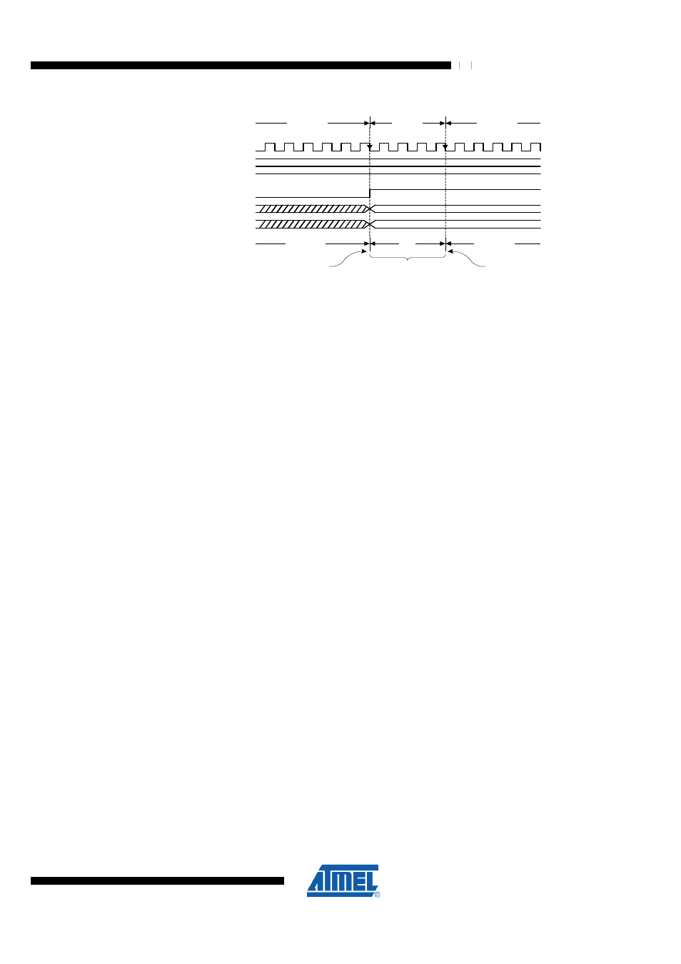
Figure 27-8. ADC Timing Diagram, Free Running Conversion
A D C C lo c k
A D T S [2 :0 ]
A D S C
A D IF
A D C H
A D C L
1 1 T
A D C _ C L K
t
T R C K
T ra c k in g
C o n v e rs io n
S ig n a n d M S B o f R e s u lt
L S B o f R e s u lt
M U X a n d R E F S U p d a te
C o n v e rs io n
C o m p le te
S a m p le & H o ld
C o n v e rs io n
0
1 1 T
A D C _C L K
27.6 Changing Channel or Reference Selection
The MUXn and REFSn bits in the ADMUX and ADCSRB Register are single buffered
through a temporary register to which the CPU has random access. This ensures that
the channels and reference selection only takes place at a safe point during the
conversion. The channel and reference selection is continuously updated either during
the AVDD power-up phase or until a conversion is started by setting ADSC. After this
the channel and reference selection is locked to ensure a sufficient initialization and
sampling time for the ADC. Continuous updating of the channel selection resumes after
the conversion has completed (ADIF in ADCSRA is set). The reference selection can
only be updated if the ADC is disabled and enabled again.
If Auto Triggering is used, the exact time of the triggering event can be undetermined.
Special care must be taken when updating the ADMUX Register, in order to control
which conversion will be affected by the new settings.
If both ADATE and ADEN in the ADSCRA Register are written to one, an interrupt
event can occur at any time. If the ADMUX Register is changed in this period, the user
cannot tell if the next conversion is based on the old or the new settings. ADMUX can
be safely updated in the following ways:
1. When ADATE or ADEN is cleared.
2. During a conversion
3. After a conversion, before the Interrupt Flag used as trigger source is cleared.
When updating ADMUX in one of these conditions, the new settings will affect the next
A/D conversion.
After the channel or reference voltage selection is updated a settling time is required for
the ADC and the gain amplifier or the reference voltage to stabilize. When changing
the channel selection while the ADC is enabled the required settling phase is
automatically inserted by the ADC interface, see section
418. For consideration on changing the reference voltage selection please refer to
section
27.6.1 Accessing the ADMUX Register
The channel selection bits MUX4:0 and MUX5 are located in two different register, the
ADMUX and the ADCSRB register. To ensure that changes go only into effect after
both register have been changed they are internally buffered (see
and
page 419). The MUX5 bit has to written first followed by a
write access to the MUX4:0 bits which triggers the update of the internal buffer. If only