6 module description, 1 receiver (rx), 1 overview – Rainbow Electronics ATmega128RFA1 User Manual
Page 74: Atmega128rfa1
74
8266A-MCU Wireless-12/09
ATmega128RFA1
Note that the received signal power as indicated by the received signal strength
indication (RSSI) value or energy detection (ED) value of the radio transceiver do not
characterize the signal quality and the ability to decode a signal.
As an example, a received signal with an input power of about 6 dB above the receiver
sensitivity likely results in a LQI value close to 255 for radio channels with very low
signal distortions. For higher signal power the LQI value becomes independent of the
actual signal strength. This is because the packet error rate for these scenarios tends
towards zero and further increased signal strength i.e. increasing the transmission
power does not decrease the error rate any further. In this case RSSI or ED can be
used to evaluate the signal strength and the link margin.
ZigBee networks often require the identification of the “best” routing between two
nodes. Both the LQI and the RSSI/ED can be used for this, dependent on the
optimization criteria. If a low packet error rate (corresponding to high throughput) is the
optimization criteria then the LQI value should be taken into consideration. If a low
transmission power or the link margin is the optimization criteria then the RSSI/ED
value is also helpful.
Combinations of LQI, RSSI and ED are possible for routing decisions. As a rule of
thumb RSSI and ED values are useful to differentiate between links with high LQI
values. Transmission links with low LQI values should be discarded for routing
decisions even if the RSSI/ED values are high. This is because RSSI and ED do not
say anything about the possibility to decode a signal. It is only an information about the
received signal strength whereas the source can be an interferer.
9.6 Module Description
9.6.1 Receiver (RX)
9.6.1.1 Overview
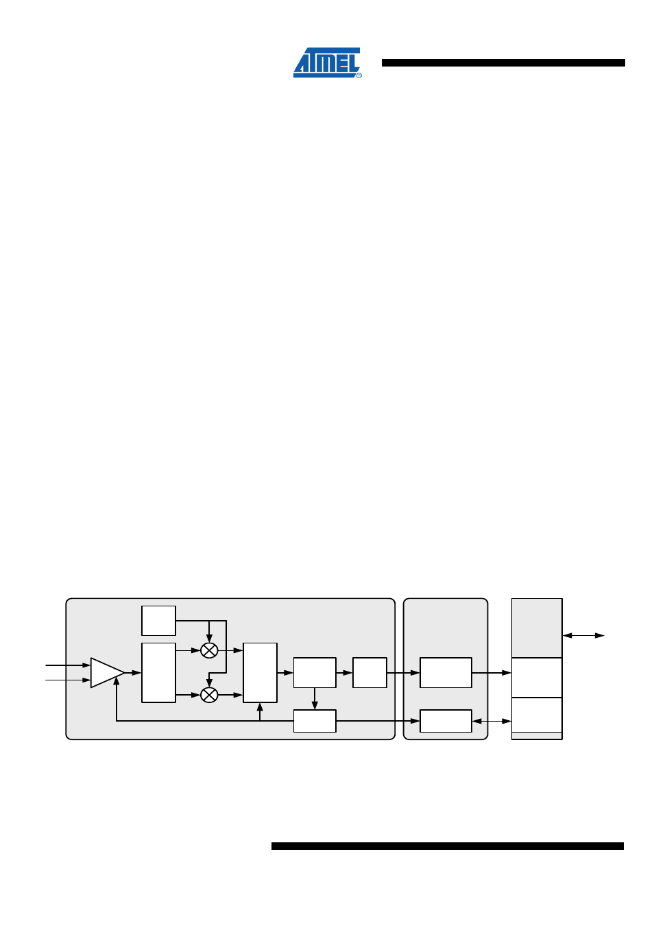
The receiver is split into an analog radio front-end and a digital base band processor
(RX BBP) according to the following figure. The digital base band processor and the
control engine are connected to the Frame Buffer and control registers which are
located in the microcontroller I/O memory space (see
and
"Transceiver to Microcontroller Interface" on page 31
).
Figure 9-20. Receiver Block Diagram
LN A
PPF
BPF
Lim iter
R X
ADC
AG C
R SSI
R FP
R FN
Analog D om ain
D igital D om ain
RX BBP
Fram e
Buffer
LO
C ontrol
µC
I/F
Registers
$01FF
$0180
$017F
$0140
I/O
M em ory
Space
The differential RF signal is amplified by a low noise amplifier (LNA), filtered (PPF) and
down converted to an intermediate frequency by a mixer. Channel selectivity is
performed using an integrated band pass filter (BPF). A limiting amplifier (Limiter)
provides sufficient gain to overcome the DC offset of the succeeding analog-to-digital