2 transmitter (tx), 1 overview, 2 frame transmit procedure – Rainbow Electronics ATmega128RFA1 User Manual
Page 76: 3 configuration, 4 tx power ramping, Atmega128rfa1
76
8266A-MCU Wireless-12/09
ATmega128RFA1
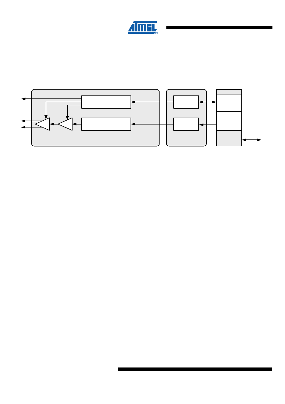
9.6.2 Transmitter (TX)
9.6.2.1 Overview
The transmitter consists of a digital base band processor (TX BBP) and an analog front
end as shown in the following figure.
Figure 9-21. Transmitter Block Diagram
PLL – TX M odulation
PA
Ext. R F front-end and
Output Power C ontrol
D IG3/4
R FP
R FN
TX D ata
Analog D om ain
TX BBP
Control
Buf
D igital Dom ain
Fram e
Buffer
µC
I/F
R egisters
I/O
M em ory
Space
$01FF
$017F
$0180
$0140
The TX BBP reads the frame data from the Frame Buffer and performs the bit-to-
symbol and symbol-to-chip mapping as specified by IEEE 802.15.4 in section 6.5.2.
The O-QPSK modulation signal is generated and fed into the analog radio front end.
The fractional-N frequency synthesizer (PLL) converts the baseband transmit signal to
the RF signal which is amplified by the power amplifier (PA). The PA output is internally
connected to bidirectional differential antenna pins (RFP, RFN) so that no external
antenna switch is needed.
9.6.2.2 Frame Transmit Procedure
The frame transmit procedure including writing PSDU data in the Frame Buffer and
initiating a transmission is described in section
"Frame Transmit Procedure" on page
.
The controller must ensure to provide valid frame data before starting the frame
transmission. For save operation, it is recommended to write the complete frame into
the Frame Buffer before starting the frame transmission.
9.6.2.3 Configuration
The maximum output power of the transmitter is typically +3.5 dBm. The output power
can be configured via the TX_PWR bits of register PHY_TX_PWR. The output power of
the transmitter can be controlled over a 20 dB range.
A transmission can be started from PLL_ON or TX_ARET_ON state by writing ‘1’ to bit
SLPTR of the TRXPR register or by writing TX_START command to the TRX_CMD bits
of register TRX_STATE.
9.6.2.4 TX Power Ramping
The PA buffer and PA are enabled sequentially to optimize the output power spectral
density (PSD). A timing example using default settings illustrates the sequence in the
next figure. In this example the transmission is initiated with the rising edge of the
SLPTR bit. The radio transceiver state changes from PLL_ON to BUSY_TX. The
modulation starts 16 µs after SLPTR.