8 serial downloading, 1 serial programming pin mapping, Atmega128rfa1 – Rainbow Electronics ATmega128RFA1 User Manual
Page 477
477
8266A-MCU Wireless-12/09
ATmega128RFA1
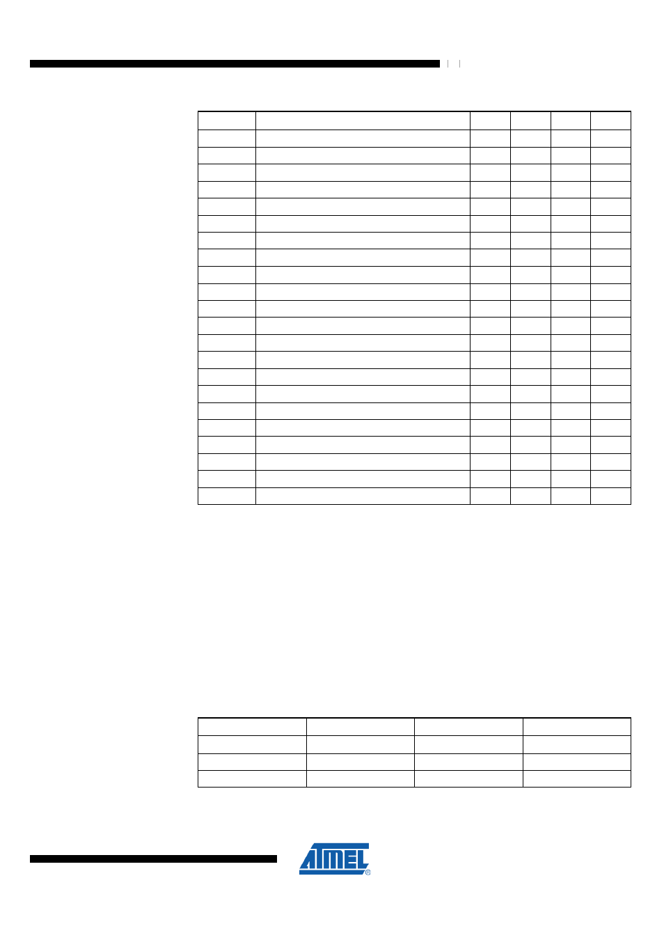
Table 31-14. Parallel Programming Characteristics, V
DEVDD
= 3.3V ± 10%
Symbol
Parameter
Min
Typ
Max
Units
t
TSTRNH
Delay TST High before RSTN High
0
ns
t
DVXH
Data and Control Valid before CLKI High
67
ns
t
XLXH
CLKI Low to CLKI High
200
ns
t
XHXL
CLKI Pulse Width High
150
ns
t
XLDX
Data and Control Hold after CLKI Low
67
ns
t
XLWL
CLKI Low to WR
___
Low
0
ns
t
XLPH
CLKI Low to PAGEL high
0
ns
t
PLXH
PAGEL low to CLKI high
150
ns
t
BVPH
BS1 Valid before PAGEL High
67
ns
t
PHPL
PAGEL Pulse Width High
150
ns
t
PLBX
BS1 Hold after PAGEL Low
67
ns
t
WLBX
BS2/1 Hold after WR
___
Low
67
ns
t
PLWL
PAGEL Low to WR
___
Low
67
ns
t
BVWL
BS2/1 Valid to WR
___
Low
67
ns
t
WLWH
WR
___
Pulse Width Low
150
ns
t
WLRL
WR
___
Low to RDY/BSY
___
Low
0
1
µs
t
WLRH
WR
___
Low to RDY/BSY
___
High
(1)
3.7
4.5
ms
t
WLRH_CE
WR
___
Low to RDY/BSY
___
High for Chip Erase
(2)
12
14.5
ms
t
XLOL
CLKI Low to OE
__
Low
0
ns
t
BVDV
BS1 Valid to DATA valid
0
250
ns
t
OLDV
OE
__
Low to DATA Valid
250
ns
t
OHDZ
OE
__
High to DATA Tri-stated
250
ns
Notes: 1. t
WLRH
is valid for the Write Flash, Write EEPROM, Write Fuse bits and Write Lock
bits commands.
2. t
WLRH_CE
is valid for the Chip Erase command.
31.8 Serial Downloading
Both the Flash and EEPROM memory arrays can be programmed using a serial
programming bus while RSTN is pulled to DVSS. The serial programming interface
consists of pins SCK, PDI (input) and PDO (output). After RSTN is set low, the
Programming Enable instruction needs to be executed first before program/erase
operations can be executed. NOTE, in
, the pin mapping for serial
programming is listed.
31.8.1 Serial Programming Pin Mapping
Table 31-15. Pin Mapping Serial Programming
Symbol
Pins
I/O
Description
PDI
PB2
I
Serial Data In
PDO
PB3
O
Serial Data Out
SCK
PB1
I
Serial Clock