Atmega128rfa1 – Rainbow Electronics ATmega128RFA1 User Manual
Page 286
286
8266A-MCU Wireless-12/09
ATmega128RFA1
COM4A1:0 bit functionality when the WGM43:0 bits are set to a normal or a CTC mode
(non-PWM). For the other functionality refer to section "Modes of Operation".
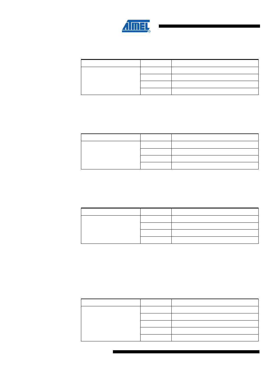
Table 18-18 COM4A Register Bits
Register Bits
Value
Description
0
Normal operation
1
Reserved
2
Reserved
COM4A1:0
3
Reserved
•
Bit 5:4 – COM4B1:0 - Compare Output Mode for Channel B
The Timer/Counter4 has only limited functionality. Therefore the COM4B1:0 bits do not
control the output compare behavior of any pin. The following table shows the
COM4B1:0 bit functionality when the WGM43:0 bits are set to a normal or a CTC mode
(non-PWM). For the other functionality refer to section "Modes of Operation".
Table 18-19 COM4B Register Bits
Register Bits
Value
Description
0
Normal operation
1
Reserved
2
Reserved
COM4B1:0
3
Reserved
•
Bit 3:2 – COM4C1:0 - Compare Output Mode for Channel C
The Timer/Counter4 has only limited functionality. Therefore the COM4C1:0 bits do not
control the output compare behavior of any pin. The following table shows the
COM4C1:0 bit functionality when the WGM43:0 bits are set to a normal or a CTC mode
(non-PWM). For the other functionality refer to section "Modes of Operation".
Table 18-20 COM4C Register Bits
Register Bits
Value
Description
0
Normal operation
1
Reserved
2
Reserved
COM4C1:0
3
Reserved
•
Bit 1:0 – WGM41:40 - Waveform Generation Mode
Combined with the WGM43:2 bits found in the TCCR4B Register, these bits control the
counting sequence of the counter, the source for maximum (TOP) counter value, and
what type of waveform generation to be used. Modes of operation supported by the
Timer/Counter unit are: Normal mode (counter), Clear Timer on Compare match (CTC)
mode, and three types of Pulse Width Modulation (PWM) modes. For more information
on the different modes see section "Modes of Operation". Note that Timer/Counter4 has
only limited functionality. It cannot be connected to any I/O pin.
Table 18-21 WGM4 Register Bits
Register Bits
Value
Description
0x0
Normal mode of operation
0x1
PWM, phase correct, 8-bit
0x2
PWM, phase correct, 9-bit
0x3
PWM, phase correct, 10-bit
WGM41:40
0x4
CTC, TOP = OCRnA