9 register description, 1 gtccr - general timer/counter control register, 2 tccr0a - timer/counter0 control register a – Rainbow Electronics ATmega128RFA1 User Manual
Page 238: Atmega128rfa1

238
8266A-MCU Wireless-12/09
ATmega128RFA1
17.9 Register Description
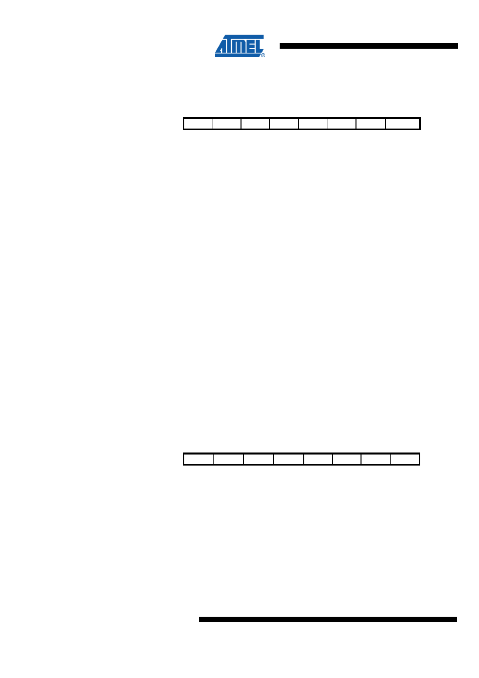
17.9.1 GTCCR – General Timer/Counter Control Register
Bit
7
6
5
4
3
2
1
0
$23 ($43)
TSM
Res4
Res3
Res2
Res1
Res0
PSRASY PSRSYNC
GTCCR
Read/Write
RW
R
R
R
R
R
R
RW
Initial Value
0
0
0
0
0
0
0
0
•
Bit 7 – TSM - Timer/Counter Synchronization Mode
Writing the TSM bit to one activates the Timer/Counter Synchronization mode. In this
mode the value that is written to the PSRASY and PSRSYNC bits is kept, hence
keeping the corresponding prescaler reset signals asserted. This ensures that the
corresponding Timer/Counters are halted and can be configured to the same value
without the risk of one of them advancing during the configuration. When the TSM bit is
written to zero, the PSRASY and PSRSYNC bits are cleared by hardware and the
Timer/Counters simultaneously start counting.
•
Bit 6:2 – Res4:0 - Reserved
This bit is reserved for future use. A read access always will return zero. A write access
does not modify the content.
•
Bit 1 – PSRASY - Prescaler Reset Timer/Counter2
When this bit is one, the Timer/Counter2 prescaler will be reset. This bit is normally
cleared immediately by hardware. If the bit is written when Timer/Counter2 is operating
in asynchronous mode, the bit will remain one until the prescaler has been reset. The
bit will not be cleared by hardware if the TSM bit is set.
•
Bit 0 – PSRSYNC - Prescaler Reset for Synchronous Timer/Counters
When this bit is one, the Timer/Counter0, Timer/Counter1, Timer/Counter3,
Timer/Counter4 and Timer/Counter5 prescaler will be reset. This bit is normally cleared
immediately by hardware, except if the TSM bit is set. Note that Timer/Counter0,
Timer/Counter1, Timer/Counter3, Timer/Counter4 and Timer/Counter5 share the same
prescaler and a reset of this prescaler will affect all timers.
17.9.2 TCCR0A – Timer/Counter0 Control Register A
Bit
7
6
5
4
3
2
1
0
$24 ($44)
COM0A1 COM0A0 COM0B1 COM0B0
Res1
Res0
WGM01 WGM00
TCCR0A
Read/Write
RW
RW
RW
RW
R
R
RW
RW
Initial Value
0
0
0
0
0
0
0
0
•
Bit 7:6 – COM0A1:0 - Compare Match Output A Mode
These bits control the Output Compare pin (OC0A) behavior. If one or both of the
COM0A1:0 bits are set, the OC0A output overrides the normal port functionality of the
I/O pin it is connected to. However, note that the Data Direction Register (DDR) bit
corresponding to the OC0A pin must be set in order to enable the output driver. When
OC0A is connected to the pin, the function of the COM0A1:0 bits depends on the
WGM02:0 bit setting. The following shows the COM0A1:0 bit functionality when the
WGM02:0 bits are set to a normal or CTC mode (non-PWM). For the functionality in
other modes refer to section "Operating Modes".
