1 basic principles of plc ladder diagram – Delta Electronics Programmable Logic Controller DVP-PLC User Manual
Page 24
1 Basic Principles of PLC Ladder Diagram
DVP-PLC Application Manual
1-20
The rising-edge differential instruction of X0 makes coil M0 generate a single pulse of ΔT (one scan cycle).
Coil Y1 will be On during this scan period. In the next scan period, coil M0 will be Off and the normally closed contact
M0 and Y1 will all be closed, making coil Y1 continue to be On until another rising-edge arrives in input X0, making
coil M0 On for another scan period and Y1 Off. Such kind of circuit relies on an input to make two actions execute
interchangeably. Also from the timing diagram on the last page, we can see that input X0 are square pulse signals of
the cycle T and coil Y1 output are square pulse signals of the cycle 2T.
Example 11: Delay circuit
T10
X0
TMR
Y1
T10
K1000
Time base: T = 0.1 sec
X0
Y1
100 seconds
When input X0 is On, due to that its corresponding normally closed contact is Off, time T10 will be Off and the
output coil Y1 will be On. T10 will be On and start to count until input X0 is Off. Output coil Y1 will be delayed for
100 seconds (K1,000 × 0.1 sec = 100 secs) and be Off. See the timing diagram above.
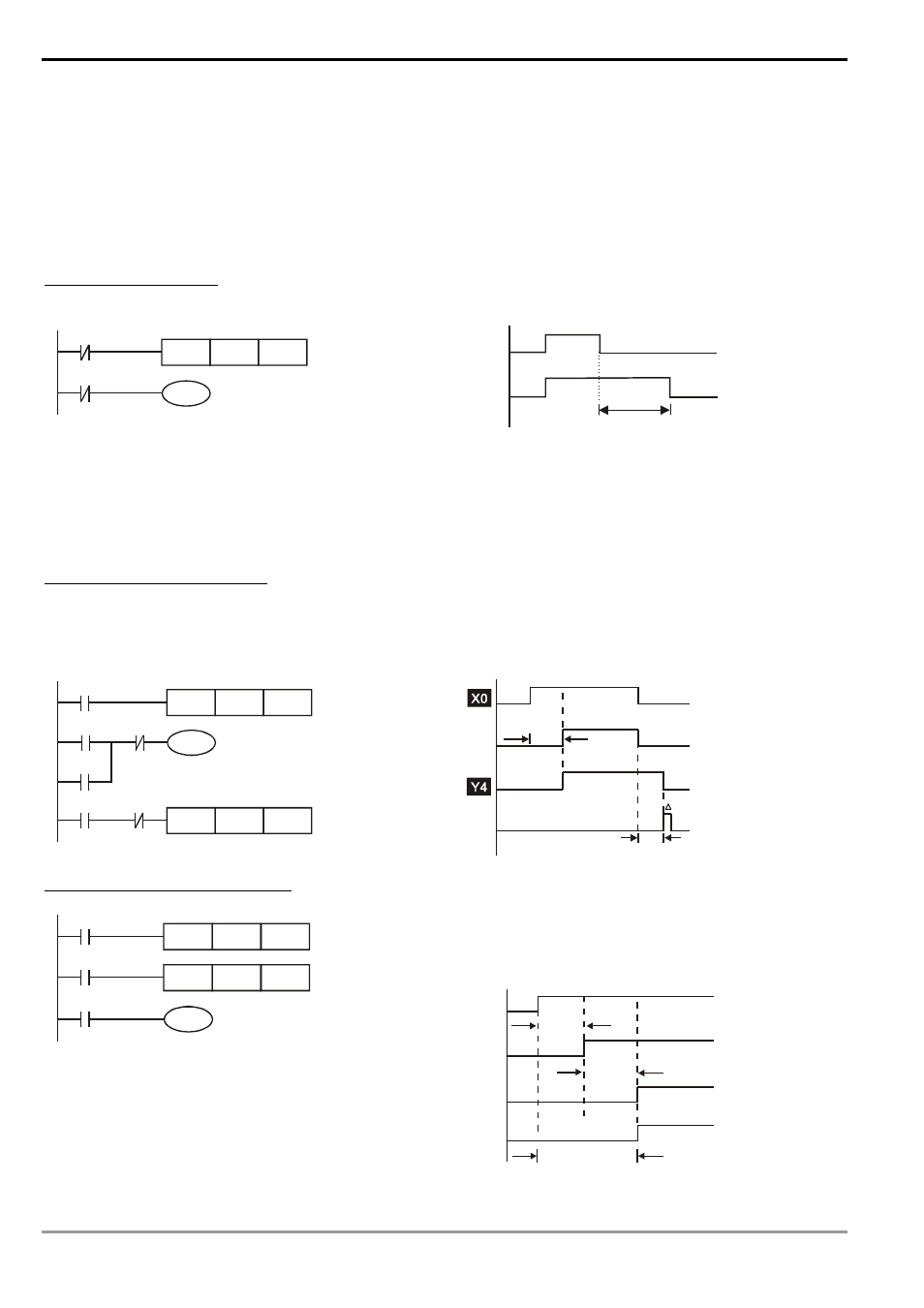
Example 12: Output delay circuit
The output delay circuit is the circuit composed of two timers. When input X0 is On and Off, output Y4 will be
delayed.
T5
T5
TMR
Y4
T6
X0
K50
Y4
T6
Y4
TMR
X0
K30
3 secs
5 secs
T5
T6
T
Example13: Timing extension circuit
T12
TMR
Kn2
T11
X0
TMR
Y1
T11
Kn1
T12
Timer = T11, T12
Clock cycle: T
The total delay time from input X0 is closed to output
Y1 is On = (n1+n2)* T. T refers to the clock cycle.
X0
Y1
T11
T12
n1*
n2*
T
T
(n1+n2)* T