4 pin layouts – HEIDENHAIN TNC 407 (243 020) Technical Manual User Manual
Page 661
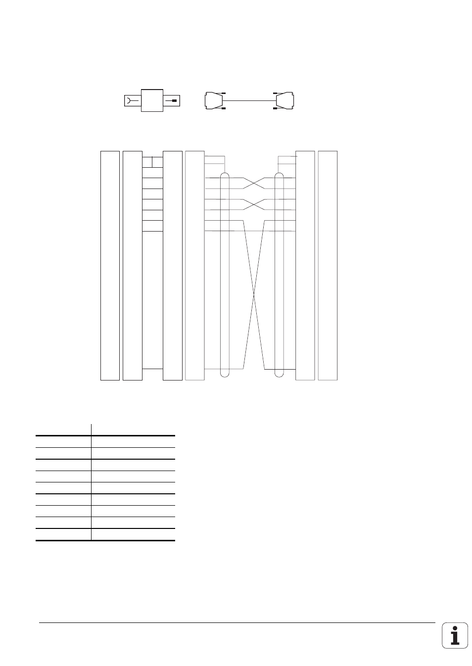
2.2.4 Pin layouts
The differences between the pin layouts of the logic unit and the adapter block of the TNC should be
noted! The corresponding pin layouts are shown below (see the "Installation and Electrical
Connection" Manual).
ws/br
WH/BN
ws/br
WH/BN
GND Chassis
RXD
TXD
CTS
RTS
DTR
GND Signal
DSR
1
2
3
4
5
6
7
8
9
10
11
12
13
14
15
16
17
18
19
20
1
2
3
4
5
6
7
8
9
10
11
12
13
14
15
16
17
18
19
20
•
•
1
2
3
4
5
6
7
8
9
10
11
12
13
14
15
16
17
18
19
20
ge
gn
rs
gr
br
rt
bl
1
2
3
4
5
6
7
8
9
10
11
12
13
14
15
16
17
18
19
20
1
2
3
4
5
6
7
8
9
10
11
12
13
14
15
16
17
18
19
20
1
2
3
4
5
6
7
8
9
10
11
12
13
14
15
16
17
18
19
20
V.24-Adapter-Block
RS-232-C
Adapter block
•
•
•
•
•
LE
Chassis GND
TXD
RXD
RTS
CTS
DSR
Signal GND
DTR
GN
YL
GY
PK
BL
RD
BN
A 9-pin plug on a PC should have the following pin layout:
Pin
Allocation
1
Not in use
2
RxD
3
TxD
4
DTR
5
GND
6
DSR
7
RTS
8
CTS
9
RI (Ring Indicator)
This manual is related to the following products: