Yaskawa MP940 User Manual
Page 168

4.7 SVA Function
4-75
4
Pn50A.0 to Pn50.B,Pn511
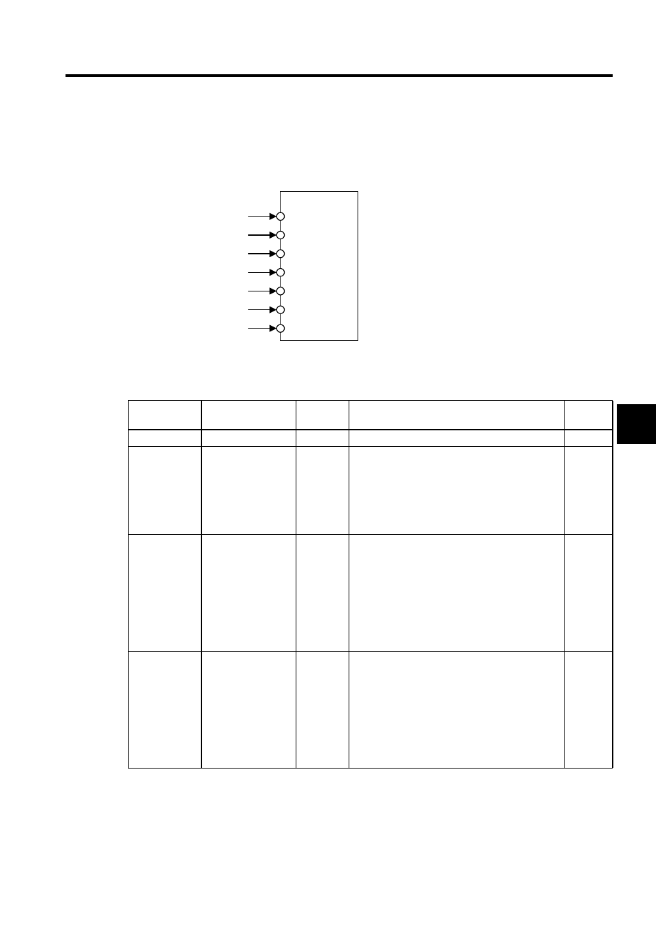
If using these parameters while connected to an MP940, set the allocation for the sequence
input signal circuit as shown below.
∗ 1.
Use the /EXT2 signal as the ZERO signal.
∗ 2.
Use the/EXT3 signal as the latch input signal.
/DEC
/P-OT
/N-OT
/EXT1
/EXT2
/EXT3
40 SI0
41 SI1
42 SI2
43 SI3
44 SI4
45 SI5
46 SI6
CN1
∗2.
∗1.
Disabled
Parameter
Name
Set Value
Details
Default
Setting
Pn50A.0
1
Any sequence input signal can be set.
0
Pn50A.1
/S-ON Signal Map-
ping
8
Signal is always disabled.
/S-ON uses a signal in shared memory.
0
Pn50A.2
/P-CON Signal Map-
ping
8
Signal is always disabled.
/P-ON uses a signal in shared memory.
1
Pn50A.3
P-OT Signal Map-
ping
2
Input the P-OT signal on the SI2 input terminal
(CN1-42). Can be disabled.
2
Pn50B.0
N-OT Signal Map-
ping
3
Input the N-OT signal on SI3 input terminal (CN1-
43). Can be disabled.
3
Pn50B.1
/ALM-RST Signal
Mapping
8
Signal is always disabled.
/ALM-RST uses a signal in shared memory.
4
Pn50B.2
/P-CL Signal Map-
ping
8
Signal is always disabled.
/P-CL uses a signal in shared memory.
5
PN50B.3
/N-CL Signal Map-
ping
8
Signal is always disabled.
/N-CL uses a signal in shared memory.
6
Pn511.0
/DEC Signal Map-
ping
1
Input /DEC signal on the SI1 input terminal (CN1-
41).
8
Pn511.1
/EXT1 Signal Map-
ping
4
Input /EXT1 signal on the SI4 input terminal (CN1-
44).
8
Pn511.2
/EXT2 Signal Map-
ping
5
Input /EXT2 signal on the SI5 input terminal (CN1-
45).
8
Pn511.3
/EXT3 Signal Map-
ping
6
Input /EXT3 signal on the SI6 input terminal (CN1-
46).
8
