Renesas SH7641 User Manual
Page 994
Section 25 Electrical Characteristics
Rev. 4.00 Sep. 14, 2005 Page 944 of 982
REJ09B0023-0400
Tc2
Tc4
Tde
Tc1
Tc3
Td1
Td2
Td3
Td4
t
CSD1
t
AD1
t
AD1
t
AD1
t
RWD1
t
RWD1
t
CSD1
t
AD1
t
AD1
t
RASD1
Read command
Column
address
t
CASD1
t
CASD1
t
BSD
t
BSD
(High)
t
DQMD1
t
DQMD1
t
DACD
t
DACD
t
RDH2
t
RDS2
t
RDH2
t
RDS2
CKIO
A25 to A0
CSn
RD/
WR
A12/A11*
1
D31 to D0
RASU/L
CASU/L
BS
CKE
DQMxx
DACKn*
2
Note:
1. An address pin to be connected to pin A10 of SDRAM.
2. Waveform for
DACKn when active low is selected.
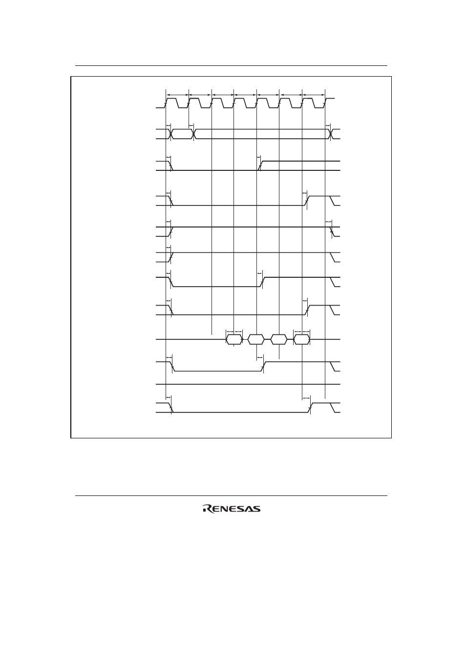
Figure 25.32 Synchronous DRAM Burst Read Bus Cycle (Four Read Cycles)
(Bank Active Mode: READ Command, Same Row Address, CAS Latency 2, WTRCD = 0 Cycle)
This manual is related to the following products:
See also other documents in the category Renesas Hardware:
- Single-Chip Microcomputer M34551T2-MCU (42 pages)
- M3T-FLX-80NRA (6 pages)
- 70 (162 pages)
- M16C/30P (102 pages)
- PROM Programming Adapter PCA7427G02 (20 pages)
- R0E572110CFK00 (40 pages)
- H8/325 Series (20 pages)
- Single-Chip Microcomputer H8/36079 (27 pages)
- Direct Dummy IC M3T-DIRECT100S (4 pages)
- M3A-2152 (95 pages)
- PCA7755D (6 pages)
- M16C/6N5 (106 pages)
- SH7085 (50 pages)
- QFP-144 (23 pages)
- H8/3834 Series (22 pages)
- RSKM16C62P (3 pages)
- H8/33937 (22 pages)
- Single-Chip Microcomputer H8SX/1622 (5 pages)
- E6000 (29 pages)
- PCA7400 (18 pages)
- PCA4738FF-64 (20 pages)
- SuperH HS7339KCU01HE (43 pages)
- M16C FAMILY (103 pages)
- PCA7412F-100 (20 pages)
- 4513 (210 pages)
- M34551E8FP (16 pages)
- Dummy IC M3T-SSOP36B-450 (4 pages)
- Emulation Pod M30100T3-RPD-E (52 pages)
- Converter Board for M30102 M30102T-PTC (4 pages)
- SH7145 (31 pages)
- HS1653ECN61H (36 pages)
- Converter Board R0E521276CFG00 (4 pages)
- PCA7302E1F-80 (18 pages)
- H8/3814 Series (21 pages)
- H8S/2646 Series (20 pages)
- SuperHTM Family SH7125 Series (40 pages)
- M30262T-PTC (4 pages)
- SH7670 (82 pages)
- H8/3864 Series (20 pages)
- Emulator System M3T-MR100 (306 pages)
- 38K0 (6 pages)
- PLQP0176KB-A (40 pages)
- Direct Dummy IC M3T-DIRECT80S (6 pages)
- PCA4738L-80A (26 pages)
- Converter Board R0E5212BACFG00 (6 pages)