Renesas SH7641 User Manual
Page 375

Section 12 Bus State Controller (BSC)
Rev. 4.00 Sep. 14, 2005 Page 325 of 982
REJ09B0023-0400
It is necessary to output the data that has been read using
RD when a buffer is established in the
data bus. The RD/
WR signal is in a read state (high output) when no access has been carried out.
Therefore, care must be taken when controlling the external data buffer, to avoid collision.
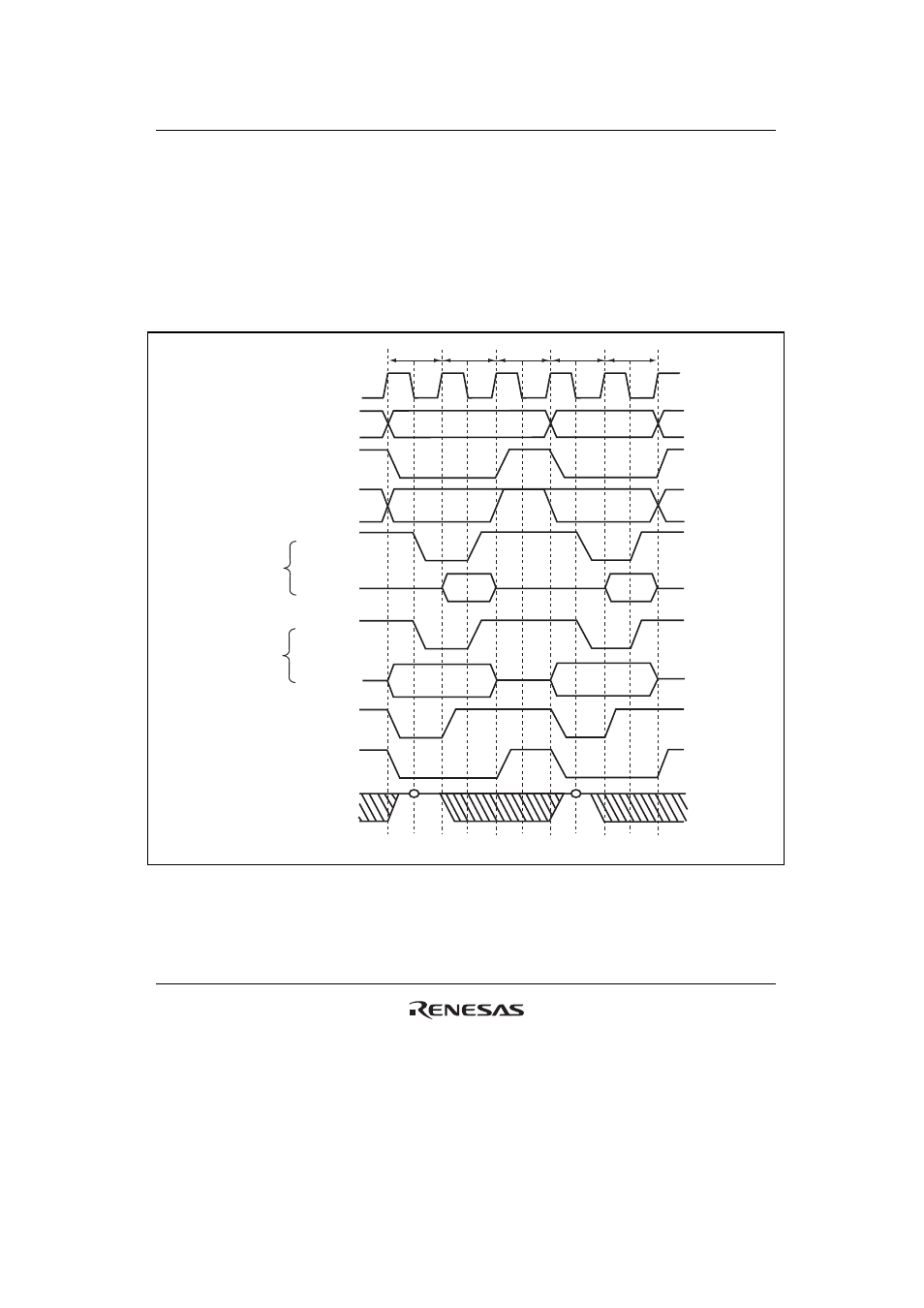
Figures 12.4 and 12.5 show the basic timings of normal space accesses. If the WM bit in
CSnWCR is cleared to 0, a Tnop cycle is inserted after the CSn space access to evaluate the
external wait (figure 12.4). If the WM bit in CSnWCR is set to 1, external waits are ignored and
no Tnop cycle is inserted (figure 12.5).
CKIO
A25 to A0
RD
RD/
WR
D15 to D0
WEn
D15 to D0
DACKn
BS
WAIT
CSn
T1 T2 Tnop T1 T2
Read
Write
*
Note: * The waveform for
DACKn is when active low is specified.
Figure 12.4 Continuous Access for Normal Space 1
Bus Width = 16 Bits, Longword Access, CSnWCR.WN Bit = 0
(Access Wait = 0, Cycle Wait = 0)
