Renesas SH7641 User Manual
Page 687
Section 18 Multi-Function Timer Pulse Unit (MTU)
Rev. 4.00 Sep. 14, 2005 Page 637 of 982
REJ09B0023-0400
buffer register for TGRA_3. At the same time, TGRC_4 functions as the buffer register for
TRGA_4, while the TCBR functions as the TCDR's buffer register.
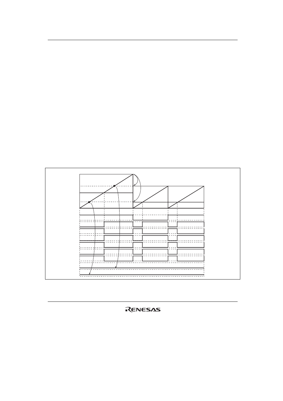
18.7.14 Reset Sync PWM Mode Buffer Operation and Compare Match Flag
When setting buffer operation for reset sync PWM mode, set the BFA and BFB bits of TMDR_4
to 0. The TIOC4C pin will be unable to produce its waveform output if the BFA bit of TMDR_4 is
set to 1.
In reset sync PWM mode, the channel 3 and channel 4 buffers operate in accordance with the BFA
and BFB bit settings of TMDR_3. For example, if the BFA bit of TMDR_3 is set to 1, TGRC_3
functions as the buffer register for TGRA_3. At the same time, TGRC_4 functions as the buffer
register for TRGA_4.
The TGFC bit and TGFD bit of TSR_3 and TSR_4 are not set when TGRC_3 and TGRD_3 are
operating as buffer registers.
Figure 18.81 shows an example of operations for TGR_3, TGR_4, TIOC3, and TIOC4, with
TMDR_3's BFA and BFB bits set to 1, and TMDR_4's BFA and BFB bits set to 0.
TGRA_3
TGRC_3
TGRB_3, TGRA_4,
TGRB_4
TGRD_3, TGRC_4,
TGRD_4
H'0000
TIOC3A
TIOC3B
TIOC3D
TIOC4A
TIOC4C
TIOC4B
TIOC4D
TGFC
TGFD
TGRA_3,
TGRC_3
TGRB_3, TGRD_3,
TGRA_4, TGRC_4,
TGRB_4, TGRD_4
Buffer transfer with
compare match A3
TCNT3
Not set
Not set
Point a
Point b
Figure 18.81 Buffer Operation and Compare-Match Flags in Reset Sync PWM Mode