9 port j, 1 register description – Renesas SH7641 User Manual
Page 912
Section 23 I/O Ports
Rev. 4.00 Sep. 14, 2005 Page 862 of 982
REJ09B0023-0400
Table 23.11 Port H Data Register (PHDR) Read/Write Operations
PHnMD2 PHnMD1 Pin
State
Read
Write
0
0
Input
Pin state
Data is written to PHDR, but does not affect
pin state.
1
Output
PHDR value Data is written to PHDR and the value is
output from the pin.
1 0 Reserved
1
Other functions Pin state
Data is written to PHDR, but does not affect
pin state.
(n = 0 to 14)
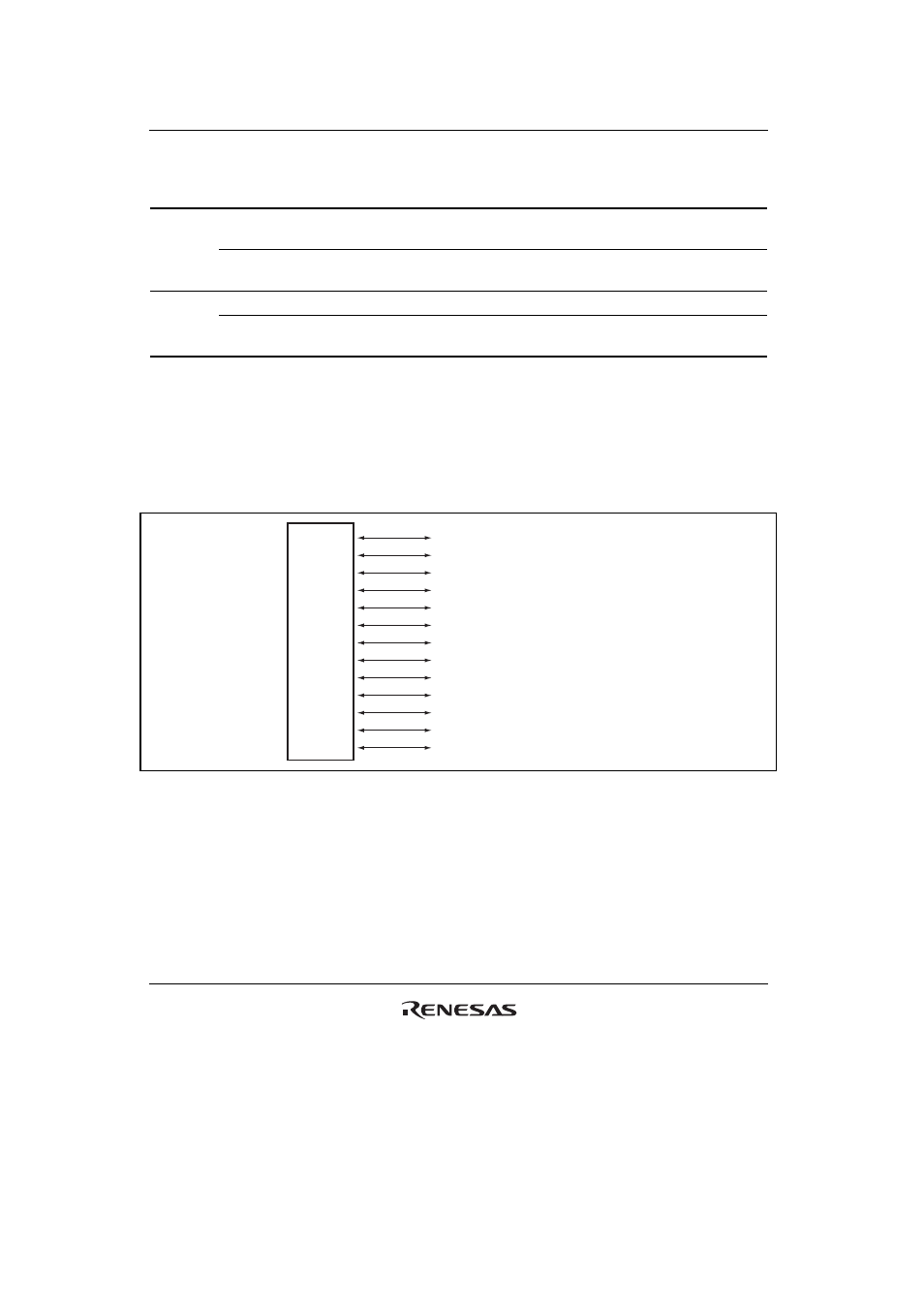
23.9 Port
J
Port J is a 13-bit input/output port with the pin configuration shown in figure 23.10. Each pin is
controlled by the port J control register (PJCR) in the PFC.
Port J
PTJ12 (input/output)/
AUDSYNC (output)
PTJ11 (input/output)/AUDATA3 (output)
PTJ10 (input/output)/AUDATA2 (output)
PTJ9 (input/output)/AUDATA1 (output)
PTJ8 (input/output)/AUDATA0 (output)
PTJ7 (input/output)/
IRQ7 (input)
PTJ6 (input/output)/
IRQ6 (input)
PTJ5 (input/output)/
IRQ5 (input)
PTJ4 (input/output)/
IRQ4 (input)
PTJ3 (input/output)/
IRQ3 (input)
PTJ2 (input/output)/
IRQ2 (input)
PTJ1 (input/output)/
IRQ1 (input)
PTJ0 (input/output)/
IRQ0 (input)
Figure 23.10 Port J
23.9.1 Register
Description
Port J has the following register.
• Port J data register (PJDR)