Renesas SH7641 User Manual
Page 416
Section 12 Bus State Controller (BSC)
Rev. 4.00 Sep. 14, 2005 Page 366 of 982
REJ09B0023-0400
Tpw
Tp
Trr
Trc
Trc
Trc
Hi-z
CKIO
A25 to A0
CSn
RD/
WR
RASL, RASU
DQMxx
D31 to D0
BS
DACKn*
2
A12/A11*
1
CASL, CASU
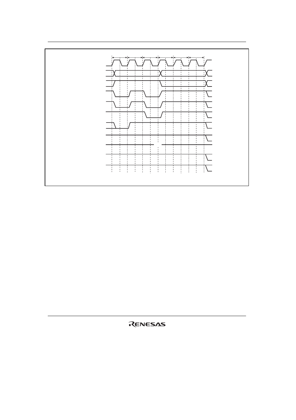
Notes: 1. Address pin to be connected to pin A10 of SDRAM.
2. The waveform for
DACKn is when active low is specified.
Figure 12.29 Auto-Refresh Timing
2. Self-refreshing
Self-refresh mode in which the refresh timing and refresh addresses are generated within the
synchronous DRAM. Self-refreshing is activated by setting both the RMODE bit and the
RFSH bit in SDCR to 1. After starting the self-refreshing, PALL command is issued in Tp
cycle after the completion of the pre-charging bank. A SELF command is then issued after
inserting idle cycles of which number is specified by the WTRP1 and WTRP0 bits in
CS3WSR. Synchronous DRAM cannot be accessed while in the self-refresh state. Self-refresh
mode is cleared by clearing the RMODE bit to 0. After self-refresh mode has been cleared,
command issuance is disabled for the number of cycles specified by the WTRC1 and WTRC0
bits in CS3WCR.