Renesas SH7641 User Manual
Page 394
Section 12 Bus State Controller (BSC)
Rev. 4.00 Sep. 14, 2005 Page 344 of 982
REJ09B0023-0400
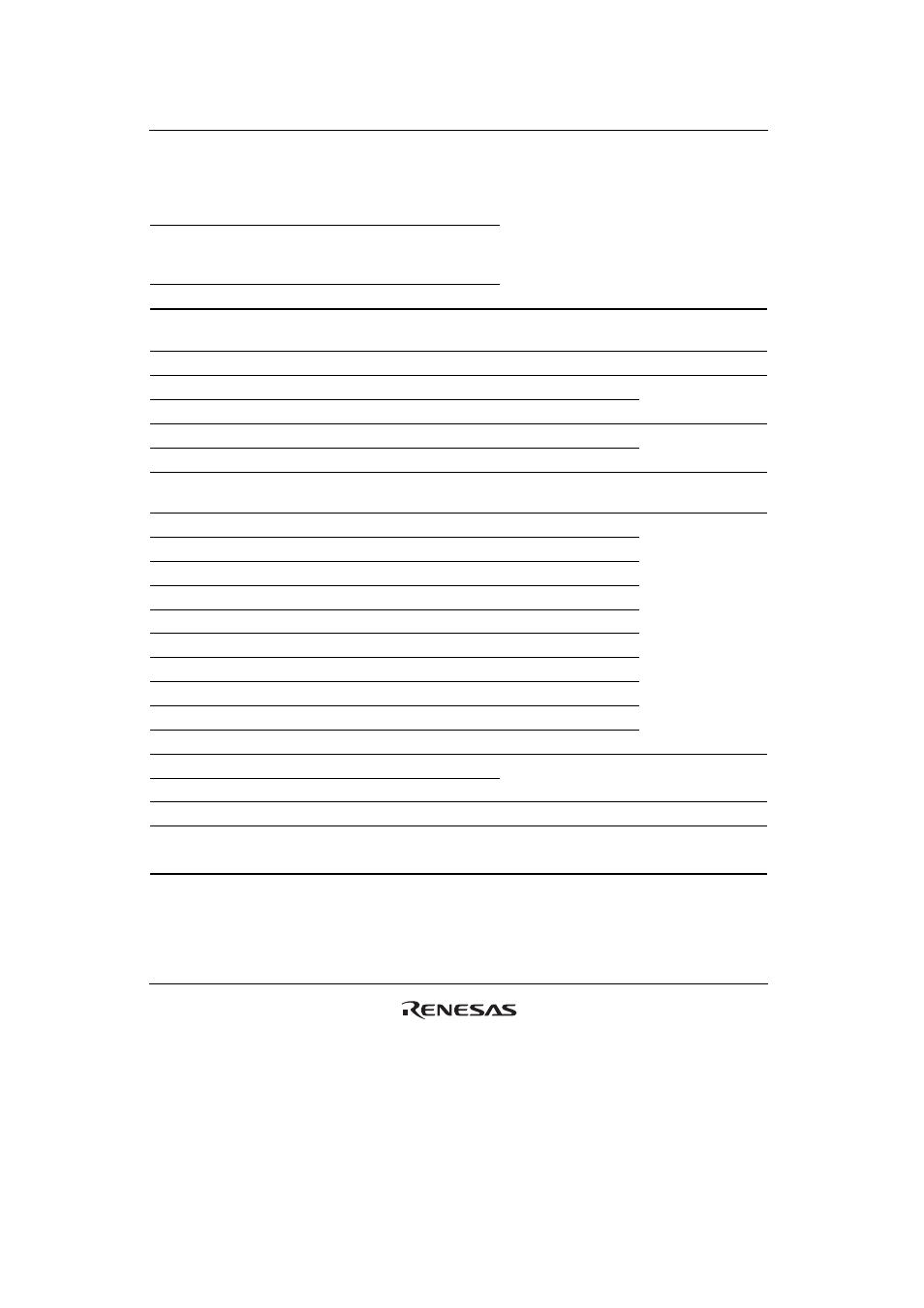
Table 12.10 Relationship between BSZ1, 0, A2/3ROW1, 0, and Address Multiplex Output
(3)
Setting
BSZ
1, 0
A2/3
ROW
1, 0
A2/3
COL
1, 0
11 (32 bits)
00 (11 bits)
00 (8 bits)
Output Pin of
This LSI
Row Address
Output Cycle
Column Address
Output Cycle
SDRAM Pin
Function
A17 A26 A17
Unused
A16 A25*
2
*
3
A25*
2
A14
(BA1)
A15 A24*
2
A24*
2
A13
(BA0)
Specifies bank
A14 A23 A14
A12
A13 A22 A13
A11
Address
A12 A21 L/H*
1
A10/AP Specifies
address/precharge
A11 A20*
2
A11
A9
A10 A19 A10
A8
A9 A18 A9
A7
A8 A17 A8
A6
A7 A16 A7
A5
A6 A15 A6
A4
A5 A14 A5
A3
A4 A13 A4
A2
A3 A12 A3
A1
A2 A11 A2
A0
Address
A1 A10 A1
A0 A9 A0
Unused
Example of connected memory
512-Mbit product (4 Mwords
× 32 bits × 4 banks, column 9 bits product): 1
256-Mbit product (4 Mwords
× 16 bits × 4 banks, column 9 bits product): 2
Notes: 1. L/H is a bit used in the command specification; it is fixed at L or H according to the
access mode.
2.
Bank
address
specification
3.
Only
the
RASL pin is asserted because the A 25 pin specified the bank address.
RASU is not asserted.