1 cache structure – Renesas SH7641 User Manual
Page 230
Section 7 Cache
Rev. 4.00 Sep. 14, 2005 Page 180 of 982
REJ09B0023-0400
7.1.1 Cache
Structure
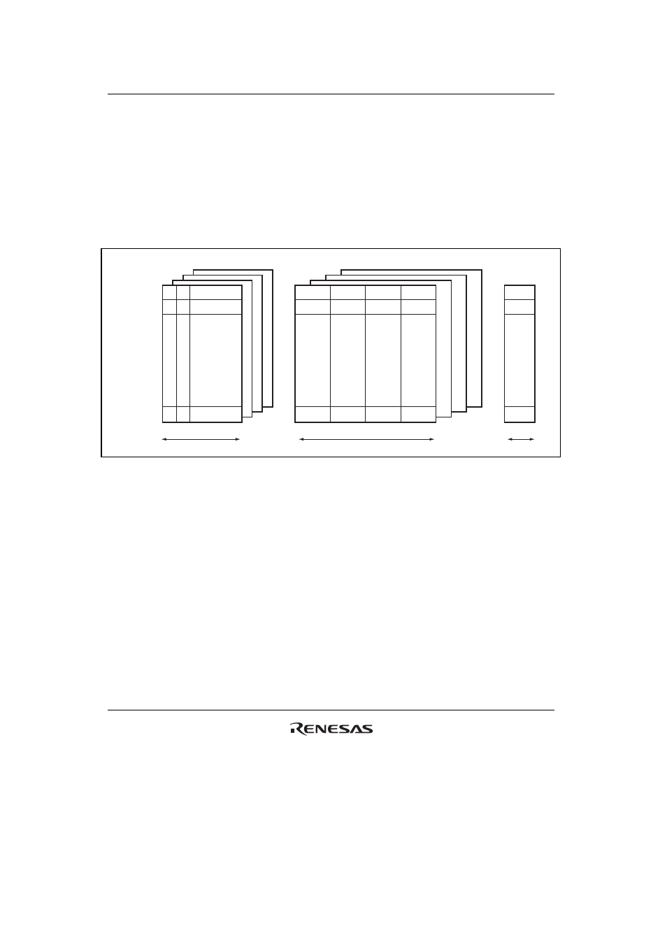
The cache mixes data and instructions and uses a 4-way set associative system. It is composed of
four ways (banks), each of which is divided into an address section and a data section. Each of the
address and data sections is divided into 256 entries. The data section of the entry is called a line.
Each line consists of 16 bytes (4 bytes
× 4). The data capacity per way is 4 kbytes (16 bytes × 256
entries), with a total of 16 kbytes in the cache as a whole (4 ways). Figure 7.1 shows the cache
structure.
24 (1 + 1 + 22) bits
128 (32
´ 4) bits
6 bits
LW0 to LW3: Longword data 0 to 3
Entry 0
Entry 1
Entry 255
0
1
255
0
1
255
V
U
Tag address
LW0
LW1
LW2
LW3
Address array (ways 0 to 3)
Data array (ways 0 to 3)
LRU
.
.
.
.
.
.
.
.
.
.
.
.
.
.
.
.
.
.
Figure 7.1 Cache Structure
Address Array: The V bit indicates whether the entry data is valid. When the V bit is 1, data is
valid; when 0, data is not valid. The U bit indicates whether the entry has been written to in write-
back mode. When the U bit is 1, the entry has been written to; when 0, it has not. The address tag
holds the physical address used in the external memory access. It is composed of 22 bits (address
bits 31 to 10) used for comparison during cache searches.
In this LSI, the top three of 32 physical address bits are used as shadow bits (see section 12, Bus
State Controller (BSC)), and therefore the top three bits of the tag address are cleared to 0.
The V and U bits are initialized to 0 by a power-on reset and retain the previous value by a manual
reset, standby mode, module standby mode, and sleep mode. The tag address is not initialized by a
power-on or manual reset, standby mode, module standby mode, and sleep mode.