Renesas SH7641 User Manual
Page 404
Section 12 Bus State Controller (BSC)
Rev. 4.00 Sep. 14, 2005 Page 354 of 982
REJ09B0023-0400
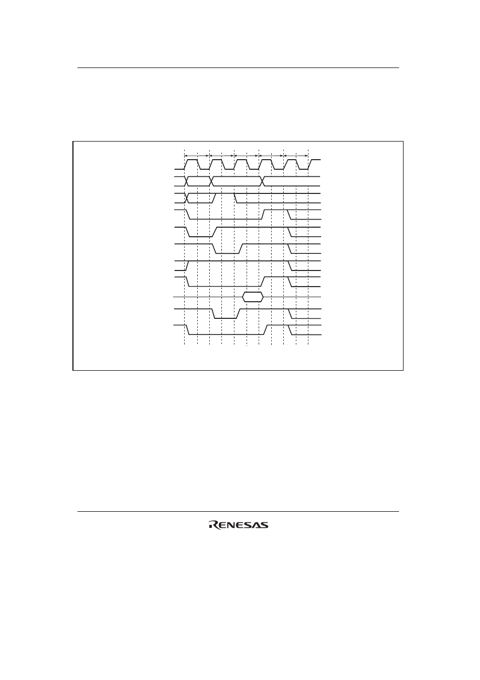
Single Read: A read access ends in one cycle when data exists in non-cacheable region and the
data bus width is larger than or equal to access size. As the burst length is set to 1 in synchronous
DRAM burst read/single write mode, only the required data is output.
Figure 12.20 shows the single read basic timing.
Tap
Tr
Tc1
Tde
Td1
CKIO
A25 to A0
CSn
RD/
WR
RASL, RASU
DQMxx
D31 to D0
BS
DACKn*
2
A12/A11*
1
CASL, CASU
Notes: 1. Address pin to be connected to pin A10 of SDRAM.
2. The waveform for
DACKn is when active low is specified.
Figure 12.20 Basic Timing for Single Read (CAS Latency 1, Auto Pre-Charge)
This manual is related to the following products: