Renesas SH7641 User Manual
Page 104
Section 2 CPU
Rev. 4.00 Sep. 14, 2005 Page 54 of 982
REJ09B0023-0400
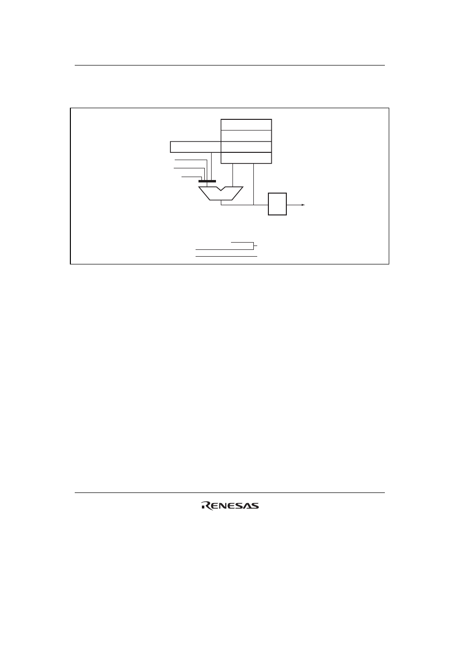
The R8 register is the index register (Is) for the address pointer (As). Single data transfer
addressing is shown in figure 2.13.
ALU
R8[Is]
R4[As]
R5[As]
–2/–4 (DEC)
+2/+4 (INC)
+0 (no update)
R3[As]
R2[As]
31
0
31
0
MAB
CAB
31
0
Note: Four address processing methods:
1. No update
2. Index register addition (Is)
3. Increment
4. Decrement
Post-increment
Pre-decrement
Figure 2.13 Single Data Transfer Addressing
Modulo Addressing: Like other DSPs, this LSI has a modulo addressing mode. Address registers
are updated in the same way in this mode. When the address pointer value reaches the preset
modulo end address, the address pointer value becomes the modulo start address.
Modulo addressing is only available for the X and Y data transfer instructions (MOVX.W and
MOVY.W). Modulo addressing mode is specified for the X address register by setting the DMX
bit in the SR register, and for the Y address register by setting the DMY bit. Modulo addressing is
valid for either the X or the Y address register, only; it cannot be set for both at the same time.
Therefore, DMX and DMY cannot both be set simultaneously. If they are, only the DMY setting
will be valid.
The MOD register is provided to set the start and end addresses of the modulo address area. The
MOD register contains MS (Modulo Start) and ME (Modulo End). An example of the use of the
MOD register (MS and ME fields) is shown below.