2 i/o buffer internal block diagram, 1 i/o buffer with weak keeper, 2 i/o buffer with open drain output – Renesas SH7641 User Manual
Page 891
Section 22 Pin Function Controller (PFC)
Rev. 4.00 Sep. 14, 2005 Page 841 of 982
REJ09B0023-0400
22.2
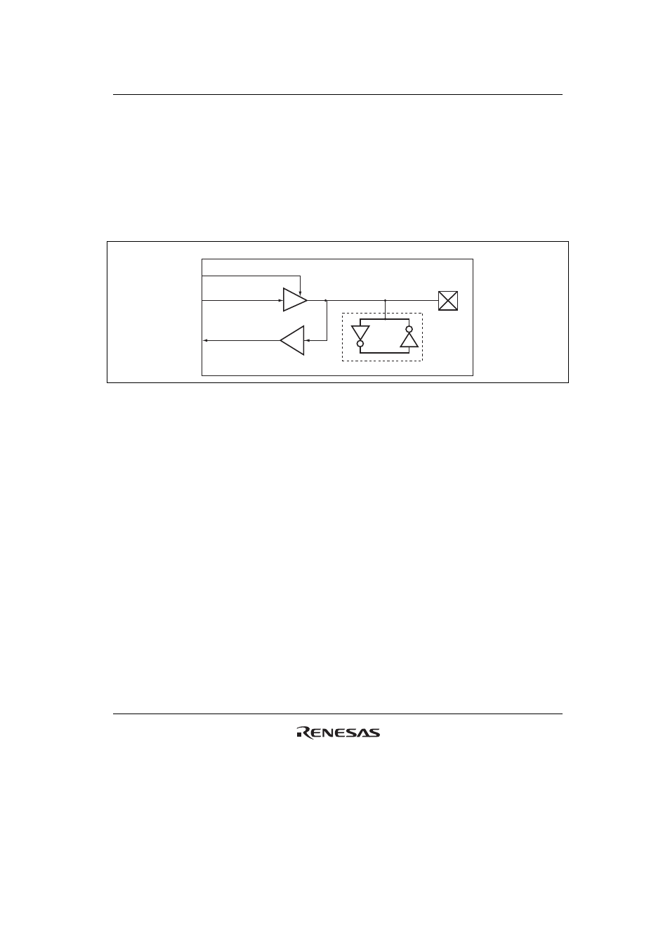
I/O Buffer Internal Block Diagram
22.2.1
I/O Buffer with Weak Keeper
All the I/O buffers except PTG10, PTG9, and PTG 7 to PTG 0 (IIC2 and analog pins) listed in
table 22.1 have weak keepers that consist of two inverters to keep the status of the pin. Figure 22.1
shows the internal block diagram of the I/O buffer.
Output enalbe
Output data
Input data
Weak keeper
I/O buffer
Figure 22.1 Internal Block Diagram of I/O Buffer with Weak Keeper
22.2.2
I/O Buffer with Open Drain Output
PTG10 and PTG9 are multiplexed with the IIC2 (SDA, SCL) pins and consist of the normal I/O
buffer and the I/O buffer with an open drain output. Setting the port G control register (PGCR) to
port input or port output enables the normal I/O buffer. Setting the PGCR to other function (IIC2)
enables the I/O buffer with an open drain output.
Figure 22.2 shows the internal block diagram of the I/O buffer with an open drain output.