Renesas SH7641 User Manual
Page 326
Section 12 Bus State Controller (BSC)
Rev. 4.00 Sep. 14, 2005 Page 276 of 982
REJ09B0023-0400
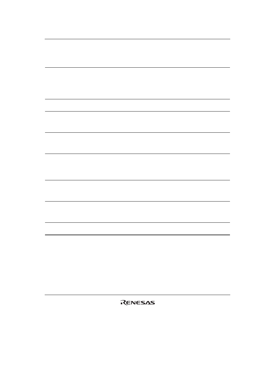
Table 12.3 Address Space Map 2 (CMNCR.MAP = 1)
Physical Address
Area
Memory to be
Connected Capacity
H'00000000 to
H'03FFFFFF
Area 0
Normal memory
Burst ROM
(Asynchronous)
Burst ROM
(Synchronous)
64 Mbytes
H'04000000 to
H'07FFFFFF
Area 1
Internal I/O register
area*
3
64 Mbytes
H'08000000 to
H'0BFFFFFF
Area 2
Normal memory
Byte-selection SRAM
SDRAM
64 Mbytes
H'0C000000 to
H'0FFFFFFF
Area 3
Normal memory
Byte-selection SRAM
SDRAM
64 Mbytes
H'10000000 to
H'13FFFFFF
Area 4
Normal memory
Byte-selection SRAM
Burst ROM
(Asynchronous)
64 Mbytes
H'14000000 to
H'17FFFFFF
Area 5*
2
Normal
memory
Byte-selection SRAM
MPX-I/O
64 Mbytes
H'18000000 to
H'1BFFFFFF
Area 6*
2
Normal
memory
Byte-selection SRAM
Burst MPX-I/O
64 Mbytes
H'1C000000 to
H'1FFFFFFF
Area 7
Reserved*
1
64
Mbytes
Notes: 1. Do not access the reserved area. If the reserved area is accessed, the correct
operation cannot be guaranteed.
2. For area 5, the CS5BBCR and CS5BWCR registers and the
CS5B signal are valid.
For area 6, the CS6BBCR and CS6BWCR registers and the
CS6B signal are valid.
3. Access the address indicated in section 24, List of Registers, for the on-chip I/O register
in area 1. Do not access area 1 addresses which are not described in the register map.
Otherwise, the correct operation cannot be guaranteed.