Renesas SH7641 User Manual
Page 67
Section 1 Overview
Rev. 4.00 Sep. 14, 2005 Page 17 of 982
REJ09B0023-0400
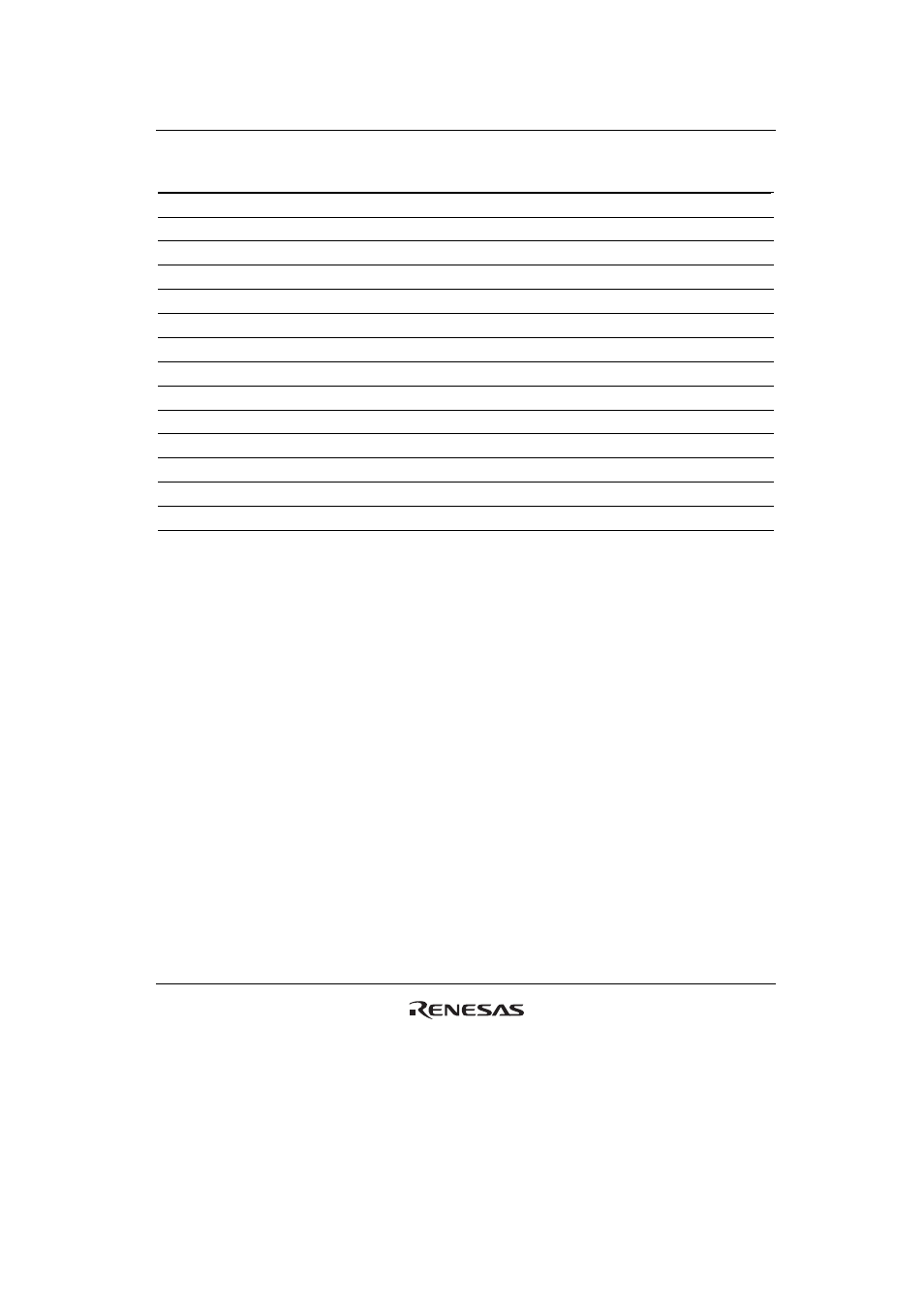
No.
(BGA256) Pin
Name
Description
C6 A1
Address
bus
A4
A0/PTA[0]
Address bus/Port A
D5
Vcc
Power supply (1.8V)
B6 D15
Data
bus
D4 Vss
Ground
(0V)
A3
VssQ
Ground for I/O circuits (0V)
B4 D14
Data
bus
A2
VccQ
Power supply for I/O circuits (3.3V)
C3 D13
Data
bus
B5 D12
Data
bus
C5 D11
Data
bus
C4 D10
Data
bus
B3 D9
Data
bus
A1 D8
Data
bus
Notes: Treatment of unused pins: All the I/O buffers except PTG10, PTG9, and PTG 7 to PTG 0
(IIC2 and analog pins) have weak keepers. Weak-keeper circuits are provided on
input/output pins, and fix the pin inputs to high or low level when the pins are not driven
externally. Unused pins that are provided weak-keeper circuits need not to be fixed their
input levels. Fix unused pins that are not provided weak-keeper circuits to high or low level.
1.
These pins are not real power supply for LSI, but each pin should be supplied each
specified voltage for correct action.
2. Weak-keeper circuits are not provided on the I/O buffer pins. Accordingly, pull the pins
up or down when they are not in use. Furthermore, do not apply intermediate voltages
to these pins when you are using them as port input pins.
3. H3 and H4 are a pair of power-supply pins located in the nearest position to the USB
module in this LSI.
Insert a bypass capacitor to the pair of pins to improve the electrical characteristic for
the USB input/output.