Renesas SH7641 User Manual
Page 198
Section 4 Clock Pulse Generator (CPG)
Rev. 4.00 Sep. 14, 2005 Page 148 of 982
REJ09B0023-0400
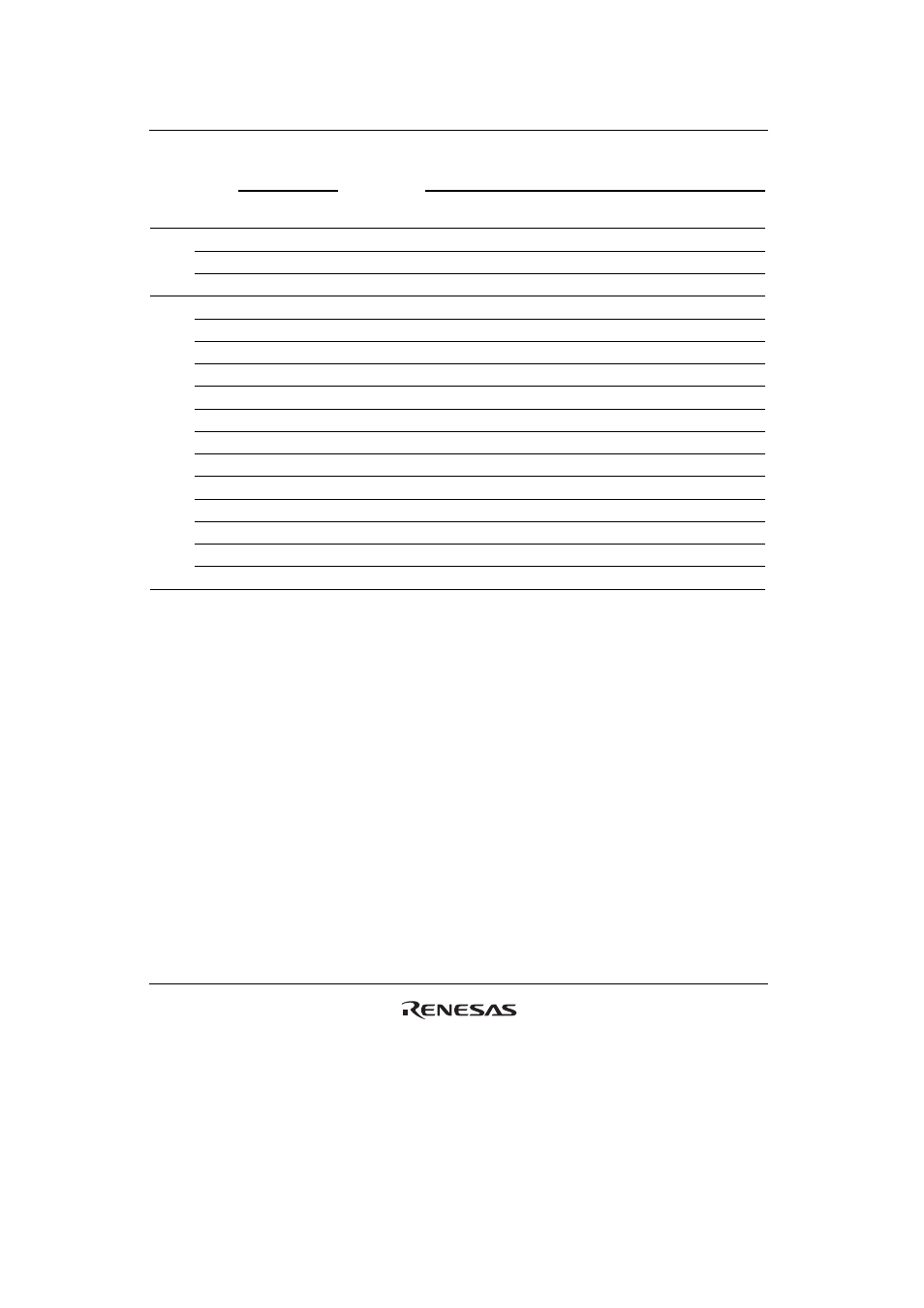
PLL frequency
multiplier Selectable
frequency ranges (MHz)
Clock
operating
mode
FRQCR
register
setting
PLL
Circuit 1
PLL
Circuit 2
Ratio of internal
clock frequencies
(I:B:P)
Input clock
Output clock
(CKIO pin)
Internal clock Bus clock
Peripheral clock
6
H'1303
ON (×4)
ON (×2)
8:2:2
10 to 12.5
20 to 25
80 to 100
20 to 25
20 to 25
H'1313
ON (×4)
ON (×2)
4:2:2
10 to 16.66
20 to 33.33
40 to 66.66
20 to 33.33
20 to 33.33
H'1333
ON (×4)
ON (×2)
2:2:2
10 to 16.66
20 to 33.33
20 to 33.33
20 to 33.33
20 to 33.33
7
H'1000
ON (×1)
OFF
1:1:1
20 to 33.33
20 to 33.33
20 to 33.33
20 to 33.33
20 to 33.33
H'1001
ON (×1)
OFF
1:1:1/2
20 to 50
20 to 50
20 to 50
20 to 50
10 to 25
H'1002
ON (×1)
OFF
1:1:1/3
20 to 50
20 to 50
20 to 50
20 to 50
6.66 to 16.66
H'1003
ON (×1)
OFF
1:1:1/4
20 to 50
20 to 50
20 to 50
20 to 50
5 to 12.5
H'1101
ON (×2)
OFF
2:1:1
20 to 33.33
20 to 33.33
40 to 66.66
20 to 33.33
20 to 33.33
H'1103
ON (×2)
OFF
2:1:1/2
20 to 50
20 to 50
40 to 100
20 to 50
10 to 25
H'1111
ON (×2)
OFF
1:1:1
20 to 33.33
20 to 33.33
20 to 33.33
20 to 33.33
20 to 33.33
H'1113
ON (×2)
OFF
1:1:1/2
20 to 50
20 to 50
20 to 50
20 to 50
10 to 25
H'1202
ON (×3)
OFF
3:1:1
26.66 to 33.33 26.66 to 33.33 80 to 100
26.66 to 33.33 26.66 to 33.33
H'1222
ON (×3)
OFF
1:1:1
26.66 to 33.33 26.66 to 33.33 26.66 to 33.33 26.66 to 33.33 26.66 to 33.33
H'1303
ON (×4)
OFF
4:1:1
20 to 25
20 to 25
80 to 100
20 to 25
20 to 25
H'1313
ON (×4)
OFF
2:1:1
20 to 33.33
20 to 33.33
40 to 66.66
20 to 33.33
20 to 33.33
H'1333
ON (×4)
OFF
1:1:1
20 to 33.33
20 to 33.33
20 to 33.33
20 to 33.33
20 to 33.33
Notes:
1. The ratio of clock frequencies, where the input clock frequency is assumed to be 1.
2. In modes 2 and 6, the frequency of the clock input from the EXTAL pin or the
frequency of the crystal resonator. In mode 7, the frequency of the clock input from
the CKIO pin.
Caution: 1. The frequency of the internal clock is the frequency of the signal input to the CKIO
pin after multiplication by the frequency-multiplier of PLL circuit 1 and division by the
divider's divisor. Do not set a frequency for the internal clock below the frequency of
the signal on the CKIO pin.
2. The frequency of the peripheral clock is the frequency of the signal input to the CKIO
pin after multiplication by the frequency-multiplier of PLL circuit 1 and division by the
divider's divisor. Set the frequency of the peripheral clock to 33.33 MHz or below. In
addition, do not set a higher frequency for the internal clock than the frequency on
the CKIO pin.
3. The frequency multiplier of the PLL circuit can be selected as x1, x2, x3 or x4. The
divisor of the divider can be selected as x1, x1/2, x1/3 or x1/4. The settings are made
in the respective frequency-control registers.
4. The signal output by PLL circuit 1 is the signal on the CKIO pin multiplied by the
frequency multiplier of PLL circuit 1. Ensure that the frequency of the signal from PLL
circuit 1 is no more than 100 MHz.