Renesas SH7641 User Manual
Page 78
Section 2 CPU
Rev. 4.00 Sep. 14, 2005 Page 28 of 982
REJ09B0023-0400
39
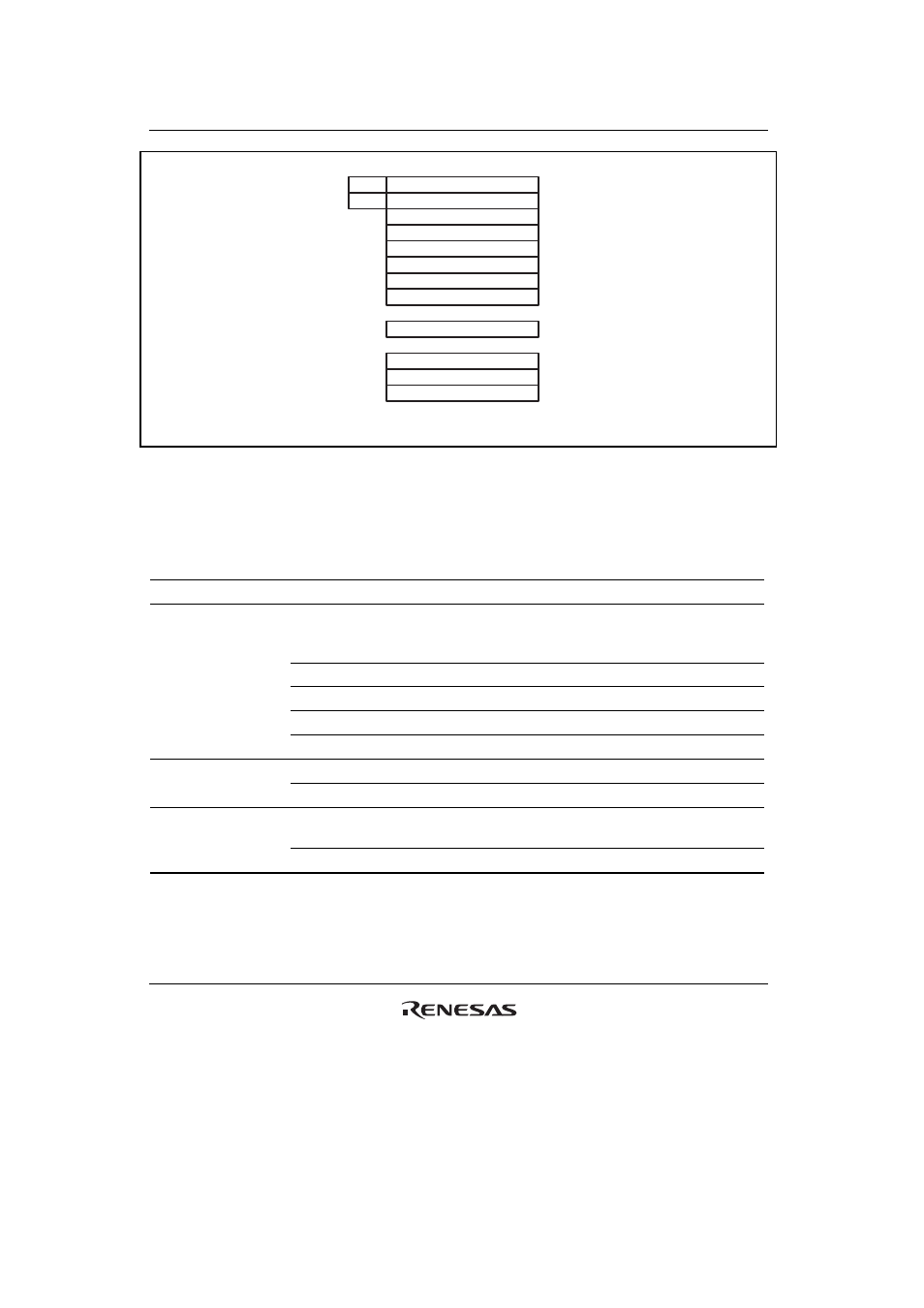
A0G
A1G
32 31
A0
A1
M0
M1
X0
X1
Y0
Y1
DSR
MS
ME
MOD
0
(c) DSP mode register configuration (DSP = 1)
Figure 2.2 Register Configuration in Each Processing Mode (2)
Register values after a reset are shown in table 2.1.
Table 2.1
Initial Register Values
Type Registers
Initial
Value
*
General registers
R0 to R15
Undefined
Control registers
SR
RB bit = 1, BL bit = 1, I3 to I0 = 1111 (H'F),
The reserved bits other than bit 30 are all 0;
bit 30 is 1, others undefined
GBR, SSR, SPC
Undefined
VBR
H'00000000
RS,
RE Undefined
MOD
Undefined
System registers
MACH, MACL, PR
Undefined
PC
H'A0000000
DSP registers
A0, A0G, A1, A1G, M0, M1,
X0, X1, Y0, Y1
Undefined
DSR
H'00000000
Note: * Initialized by a power-on or manual reset.