1 block diagram, Figure 21.1 block diagram of a/d converter – Renesas SH7641 User Manual
Page 848
Section 21 A/D Converter
Rev. 4.00 Sep. 14, 2005 Page 798 of 982
REJ09B0023-0400
21.1.1 Block
Diagram
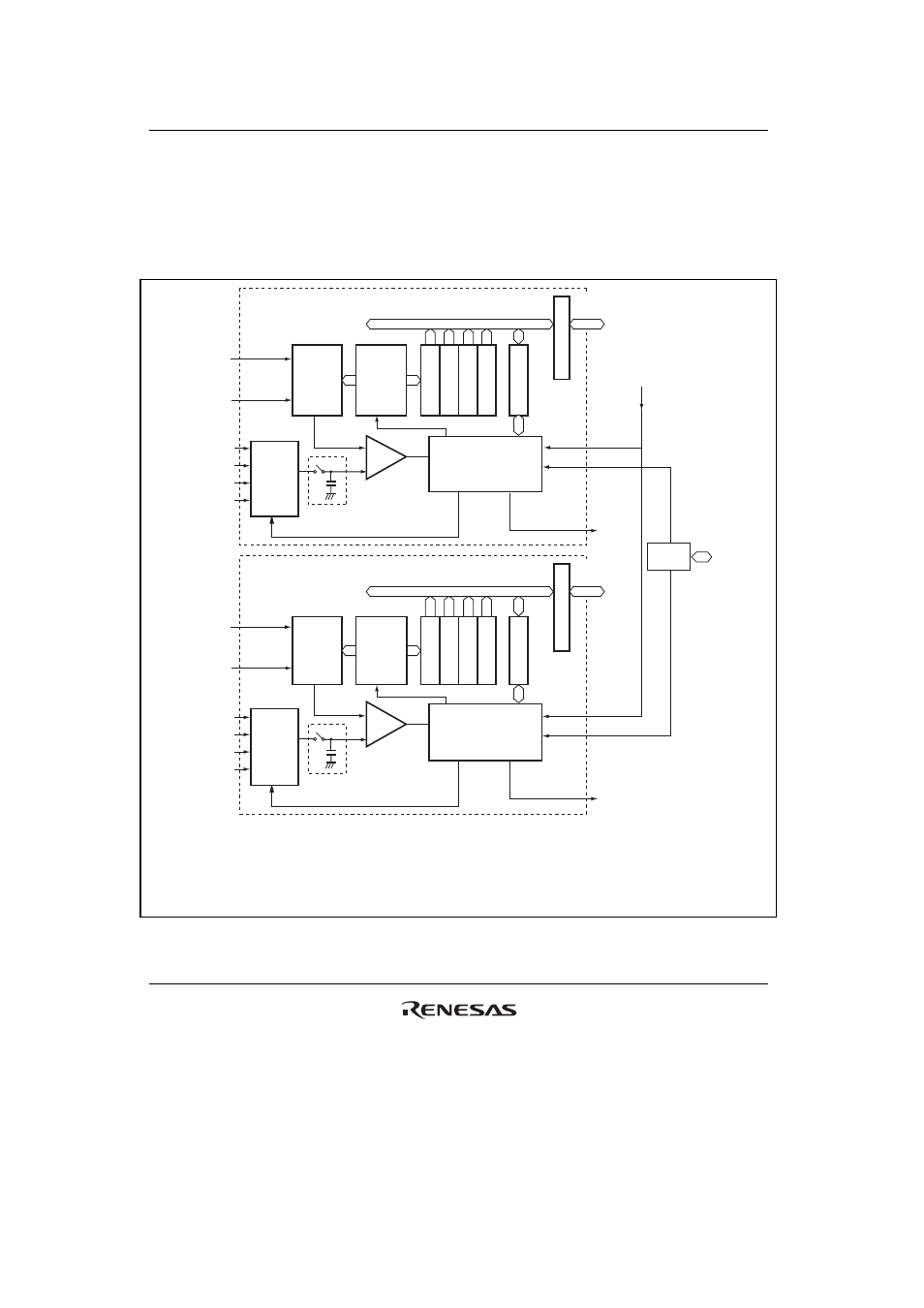
Figure 21.1 shows a block diagram of the A/D converter.
AVcc and AVss for both A/D modules are common pins in the chip.
ADI0
interrupt
signal
ADCSR 0:
ADDRA 0:
ADDRB 0:
ADDRC 0:
ADDRD 0:
ADCR:
[Legend]
A/D 0 control/status register
A/D 0 data register A
A/D 0 data register B
A/D 0 data register C
A/D 0 data register D
A/D0, A/D1 control register
ADCSR 1:
ADDRA 1:
ADDRB 1:
ADDRC 1:
ADDRD 1:
A/D 1 control/status register
A/D 1 data register A
A/D 1 data register B
A/D 1 data register C
A/D 1 data register D
10 bit
A/D
ADDRA1
ADDRB1
ADDRC1
ADDRD1
Bus interface bus
Peripheral data bus
Analog
multi
plecer
Control circuit
Successive
approxi- mation
register
+
–
Comparator
Sample and-
hold circuit
ADI1
interrupt
signal
AV
SS
AN4
AN5
AN6
AN7
AN0
AN1
AN2
AN3
ADCSR1
AV
CC
A/D converter 1
Internal
data bus
10 bit
A/D
ADDRA0
ADDRB0
ADDRC0
ADDRD0
Bus interface bus
Peripheral data bus
Analog
multi
plecer
Control circuit
Successive
approxi- mation
register
+
–
Comparator
Sample and-
hold circuit
MTU
trigger
AV
SS
ADCSR0
AV
CC
A/D converter 0
Internal
data bus
ADCR
Figure 21.1 Block Diagram of A/D Converter