Renesas SH7641 User Manual
Page 644
Section 18 Multi-Function Timer Pulse Unit (MTU)
Rev. 4.00 Sep. 14, 2005 Page 594 of 982
REJ09B0023-0400
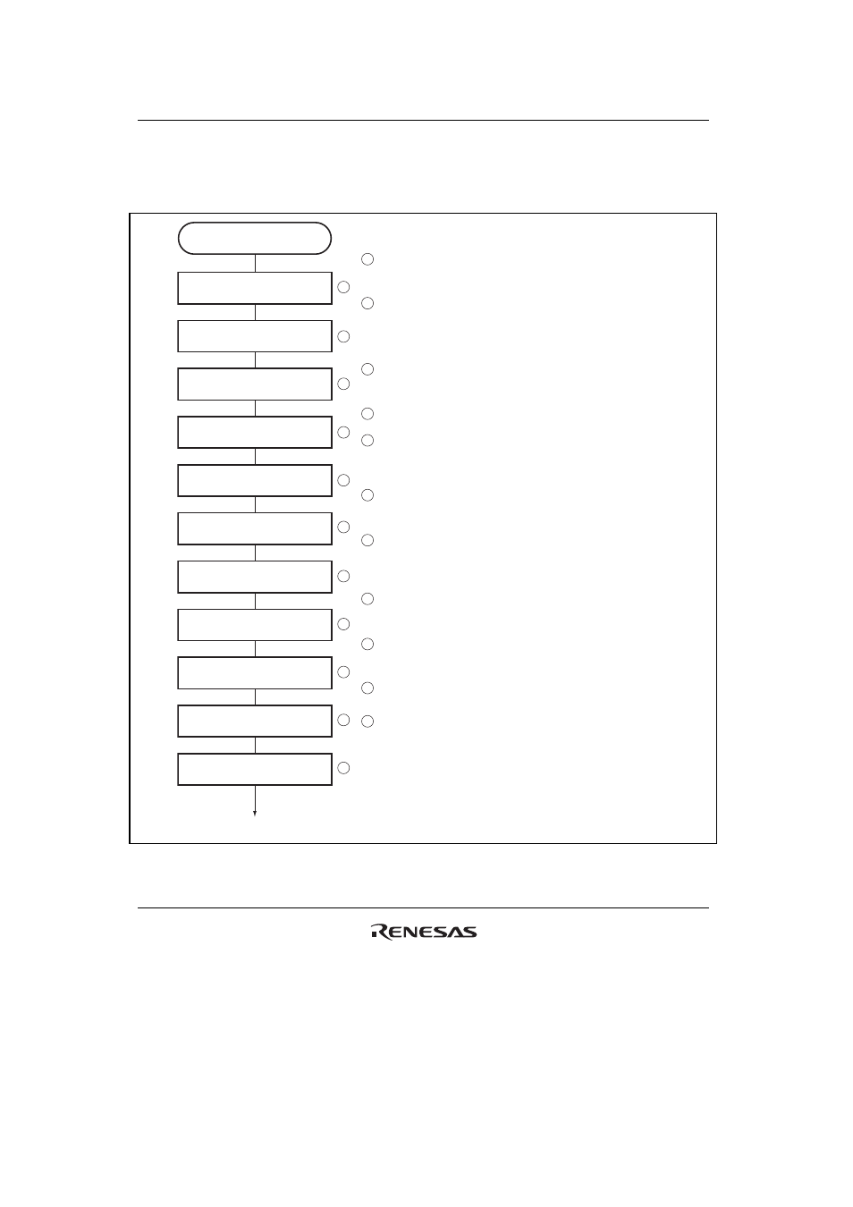
Example of Complementary PWM Mode Setting Procedure
An example of the complementary PWM mode setting procedure is shown in figure 18.33.
Complementary PWM mode
Stop count operation
Counter clock, counter clear
source selection
Brushless DC motor control
setting
TCNT setting
Inter-channel synchronization
setting
TGR setting
Dead time, carrier cycle
setting
PWM cycle output enabling,
PWM output level setting
Complementary PWM mode
setting
3
Enable waveform output
Start count operation
2
4
5
6
7
8
9
10
11
1
3
2
4
5
6
7
8
9
10
11
1 Clear bits CST3 and CST4 in the timer start register (TSTR) to 0, and
halt timer counter (TCNT) operation. Perform complementary PWM
mode setting when TCNT_3 and TCNT_4 are stopped.
Set the same counter clock and clock edge for channels 3 and 4 with
bits TPSC2 to TPSC0 and bits CKEG1 and CKEG0 in the timer
control register (TCR). Use bits CCLR2 to CCLR0 to set synchronous
clearing only when restarting by a synchronous clear from another
channel during complementary PWM mode operation.
When performing brushless DC motor control, set bit BDC in the
timer gate control register (TGCR) and set the feedback signal input
source and output chopping or gate signal direct output.
Set the dead time in TCNT_3. Set TCNT_4 to H'0000.
Set only when restarting by a synchronous clear from another
channel during complementary PWM mode operation. In this case,
synchronize the channel generating the synchronous clear with
channels 3 and 4 using the timer synchro register (TSYR).
Set the output PWM duty in the duty registers (TGRB_3, TGRA_4,
TGRB_4) and buffer registers (TGRD_3, TGRC_4, TGRD_4). Set the
same initial value in each corresponding TGR.
Set the dead time in the dead time register (TDDR), 1/2 the carrier
cycle in the carrier cycle data register (TCDR) and carrier cycle buffer
register (TCBR), and 1/2 the carrier cycle plus the dead time in
TGRA_3 and TGRC_3.
Select enabling/disabling of toggle output synchronized with the PWM
cycle using bit PSYE in the timer output control register (TOCR), and
set the PWM output level with bits OLSP and OLSN.
Select complementary PWM mode in timer mode register 3
(TMDR_3). Pins TIOC3A, TIOC3B, TIOC3D, TIOC4A, TIOC4B,
TIOC4C, and TIOC4D function as output pins. Do not set in TMDR_4.
Set enabling/disabling of PWM waveform output pin output in the
timer output master enable register (TOER).
Set bits CST3 and CST4 in TSTR to 1 simultaneously to start the
count operation.
Figure 18.33 Example of Complementary PWM Mode Setting Procedure