Figure 16.15 receive mode operation timing – Renesas SH7641 User Manual
Page 550
Section 16 I
2
C Bus Interface 2 (IIC2)
Rev. 4.00 Sep. 14, 2005 Page 500 of 982
REJ09B0023-0400
1
2
7
8
1
7
8
1
2
SCL
MST
TRS
RDRF
ICDRS
ICDRR
SDA
(Input)
Bit 0
Bit 6
Bit 7
Bit 0
Bit 6
Bit 7
Bit 0
Bit 1
Bit 1
User
processing
Data 1
Data 1
Data 2
Data 2
Data 3
[2] Set MST
(when outputting the clock)
[3] Read ICDRR
[3] Read ICDRR
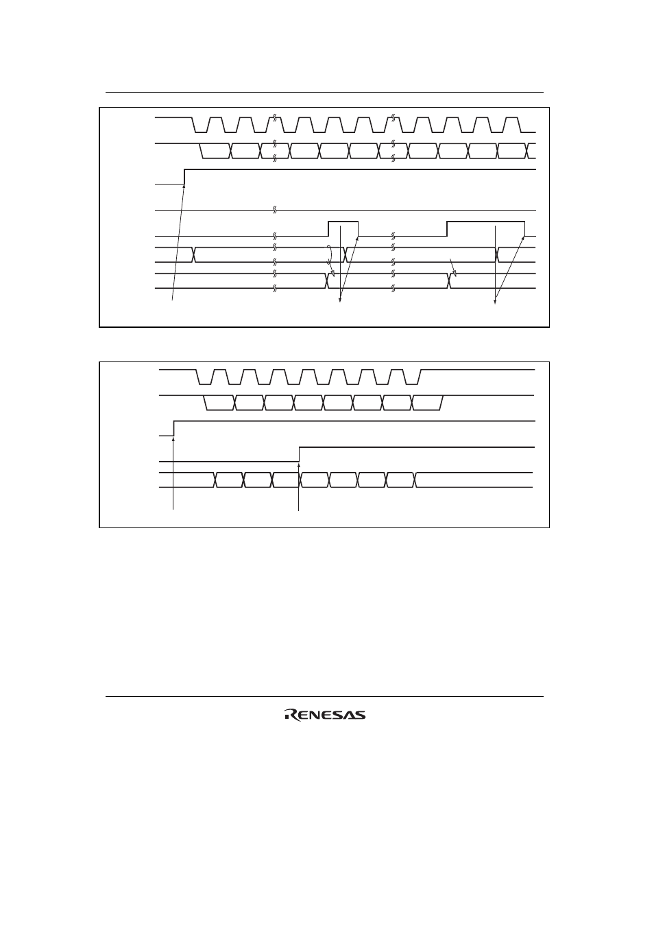
Figure 16.15 Receive Mode Operation Timing
SDA
(Input)
Bit 0
1
2
3
4
5
6
7
8
000
Bit 1
Bit 2
Bit 3
Bit 4
Bit 5
Bit 6
Bit 7
SCL
MST
RCVD
BC2 to BC0
[2] Set MST
111
110
101
100
011
010
001
000
[3] Set the RCVD bit after checking if BSC2 = 1
Figure 16.16 Operation Timing For Receiving One Byte
This manual is related to the following products:
See also other documents in the category Renesas Hardware:
- Single-Chip Microcomputer M34551T2-MCU (42 pages)
- M3T-FLX-80NRA (6 pages)
- 70 (162 pages)
- M16C/30P (102 pages)
- PROM Programming Adapter PCA7427G02 (20 pages)
- R0E572110CFK00 (40 pages)
- H8/325 Series (20 pages)
- Single-Chip Microcomputer H8/36079 (27 pages)
- Direct Dummy IC M3T-DIRECT100S (4 pages)
- M3A-2152 (95 pages)
- PCA7755D (6 pages)
- M16C/6N5 (106 pages)
- SH7085 (50 pages)
- QFP-144 (23 pages)
- H8/3834 Series (22 pages)
- RSKM16C62P (3 pages)
- H8/33937 (22 pages)
- Single-Chip Microcomputer H8SX/1622 (5 pages)
- E6000 (29 pages)
- PCA7400 (18 pages)
- PCA4738FF-64 (20 pages)
- SuperH HS7339KCU01HE (43 pages)
- M16C FAMILY (103 pages)
- PCA7412F-100 (20 pages)
- 4513 (210 pages)
- M34551E8FP (16 pages)
- Dummy IC M3T-SSOP36B-450 (4 pages)
- Emulation Pod M30100T3-RPD-E (52 pages)
- Converter Board for M30102 M30102T-PTC (4 pages)
- SH7145 (31 pages)
- HS1653ECN61H (36 pages)
- Converter Board R0E521276CFG00 (4 pages)
- PCA7302E1F-80 (18 pages)
- H8/3814 Series (21 pages)
- H8S/2646 Series (20 pages)
- SuperHTM Family SH7125 Series (40 pages)
- M30262T-PTC (4 pages)
- SH7670 (82 pages)
- H8/3864 Series (20 pages)
- Emulator System M3T-MR100 (306 pages)
- 38K0 (6 pages)
- PLQP0176KB-A (40 pages)
- Direct Dummy IC M3T-DIRECT80S (6 pages)
- PCA4738L-80A (26 pages)
- Converter Board R0E5212BACFG00 (6 pages)