Renesas SH7641 User Manual
Page 414
Section 12 Bus State Controller (BSC)
Rev. 4.00 Sep. 14, 2005 Page 364 of 982
REJ09B0023-0400
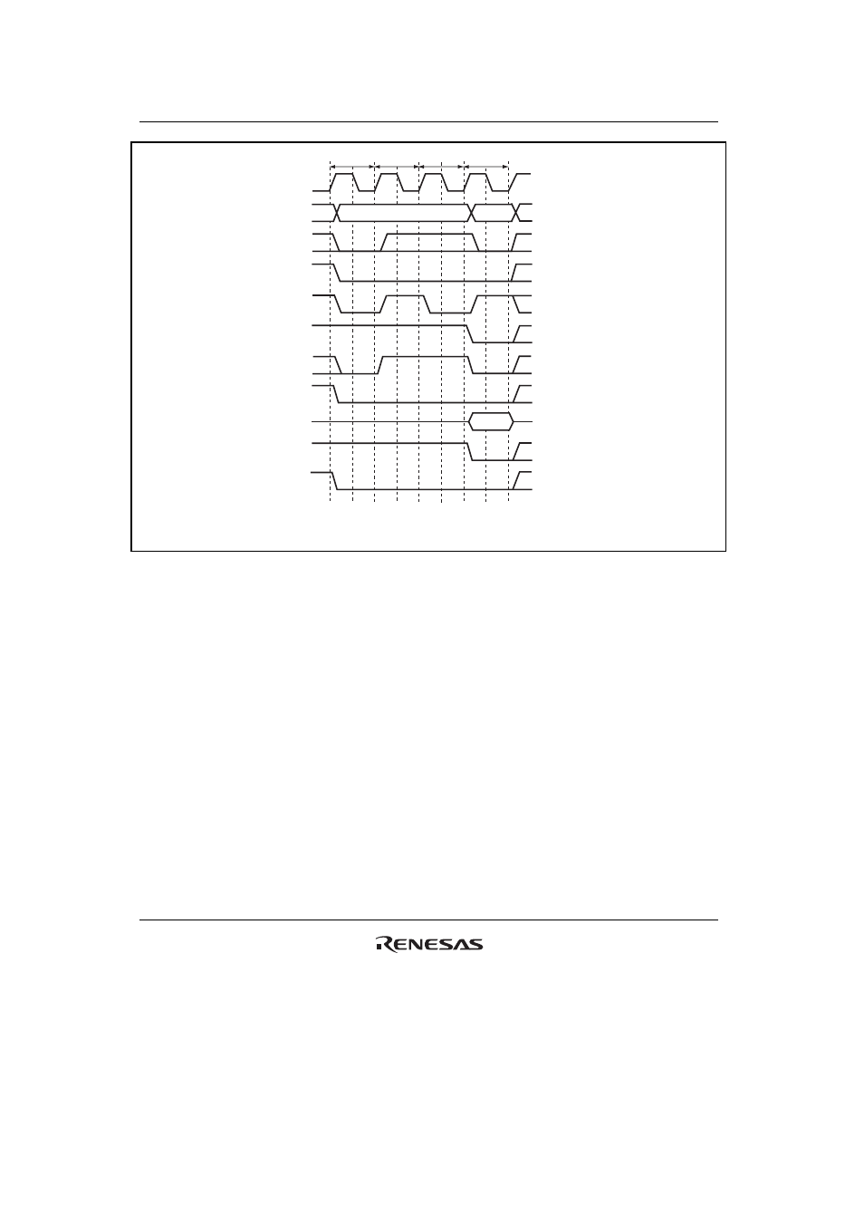
Tpw
Tp
Tc1
Tr
CKIO
A25 to A0
CSn
RD/
WR
RASL, RASU
DQMxx
D31 to D0
BS
DACKn*
2
A12/A11*
1
CASL, CASU
Notes: 1. Address pin to be connected to pin A10 of SDRAM.
2. The waveform for
DACKn is when active low is specified.
Figure 12.28 Single Write Timing
(Bank Active, Different Row Addresses in the Same Bank)
Refreshing: This LSI has a function for controlling synchronous DRAM refreshing. Auto-
refreshing can be performed by clearing the RMODE bit to 0 and setting the RFSH bit to 1 in
SDCR. A continuous refreshing can be performed by setting the RRC2 to RRC0 bits in RTCSR. If
synchronous DRAM is not accessed for a long period, self-refresh mode, in which the power
consumption for data retention is low, can be activated by setting both the RMODE bit and the
RFSH bit to 1.