Figure 25.11 bus release timing, Figure 25.12 pin driving timing in standby mode – Renesas SH7641 User Manual
Page 972
Section 25 Electrical Characteristics
Rev. 4.00 Sep. 14, 2005 Page 922 of 982
REJ09B0023-0400
CKIO
(HIZCNT = 1)
BREQ
BACK
A25 to A0,
D31 to D0
RD, RD/WR,
RASU/L,
CASU/L,
CSn, WEn,
BS, CKE
CKIO
(HIZCNT = 0)
BREQH
t
BOFF2
t
BREQS
t
BACKD
t
BACKD
t
BREQH
t
BREQS
t
BON1
t
BOFF1
t
BOFF2
t
BON2
t
BON2
t
When
HZCNT = 1
When
HZCNT = 0
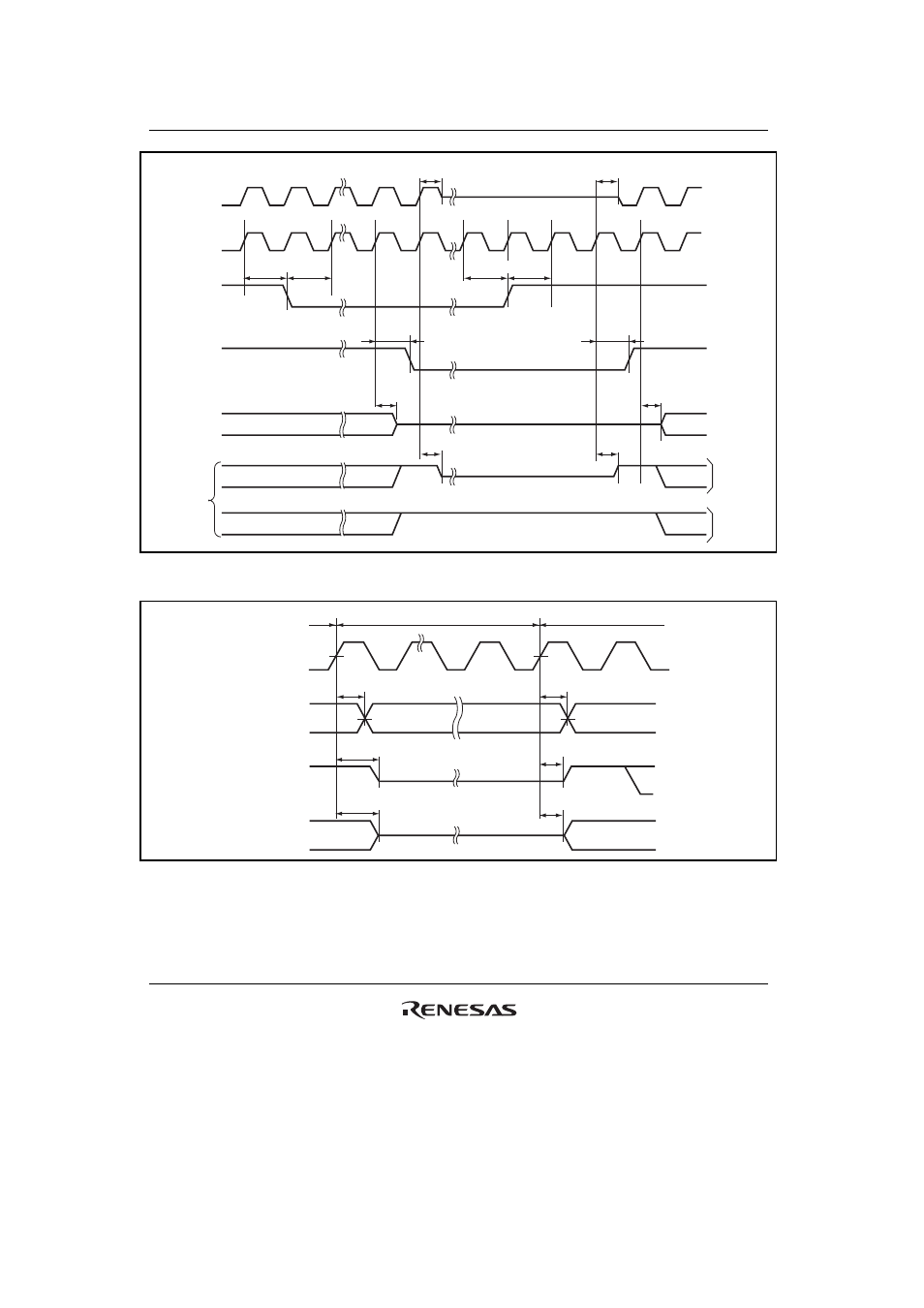
Figure 25.11 Bus Release Timing
CKIO input
t
STD
t
BOFF2
t
BOFF1
t
STD
t
BON2
t
BON1
Normal mode
Standby mode
Normal mode
STATUS 0
STATUS 1
A25 to A0,
D31 to D0
RD, RD/WR,
RASU/L,
CASU/L,
CSn, WEn,
BS, CKE
Figure 25.12 Pin Driving Timing in Standby Mode
This manual is related to the following products:
See also other documents in the category Renesas Hardware:
- Single-Chip Microcomputer M34551T2-MCU (42 pages)
- M3T-FLX-80NRA (6 pages)
- 70 (162 pages)
- M16C/30P (102 pages)
- PROM Programming Adapter PCA7427G02 (20 pages)
- R0E572110CFK00 (40 pages)
- H8/325 Series (20 pages)
- Single-Chip Microcomputer H8/36079 (27 pages)
- Direct Dummy IC M3T-DIRECT100S (4 pages)
- M3A-2152 (95 pages)
- PCA7755D (6 pages)
- M16C/6N5 (106 pages)
- SH7085 (50 pages)
- QFP-144 (23 pages)
- H8/3834 Series (22 pages)
- RSKM16C62P (3 pages)
- H8/33937 (22 pages)
- Single-Chip Microcomputer H8SX/1622 (5 pages)
- E6000 (29 pages)
- PCA7400 (18 pages)
- PCA4738FF-64 (20 pages)
- SuperH HS7339KCU01HE (43 pages)
- M16C FAMILY (103 pages)
- PCA7412F-100 (20 pages)
- 4513 (210 pages)
- M34551E8FP (16 pages)
- Dummy IC M3T-SSOP36B-450 (4 pages)
- Emulation Pod M30100T3-RPD-E (52 pages)
- Converter Board for M30102 M30102T-PTC (4 pages)
- SH7145 (31 pages)
- HS1653ECN61H (36 pages)
- Converter Board R0E521276CFG00 (4 pages)
- PCA7302E1F-80 (18 pages)
- H8/3814 Series (21 pages)
- H8S/2646 Series (20 pages)
- SuperHTM Family SH7125 Series (40 pages)
- M30262T-PTC (4 pages)
- SH7670 (82 pages)
- H8/3864 Series (20 pages)
- Emulator System M3T-MR100 (306 pages)
- 38K0 (6 pages)
- PLQP0176KB-A (40 pages)
- Direct Dummy IC M3T-DIRECT80S (6 pages)
- PCA4738L-80A (26 pages)
- Converter Board R0E5212BACFG00 (6 pages)