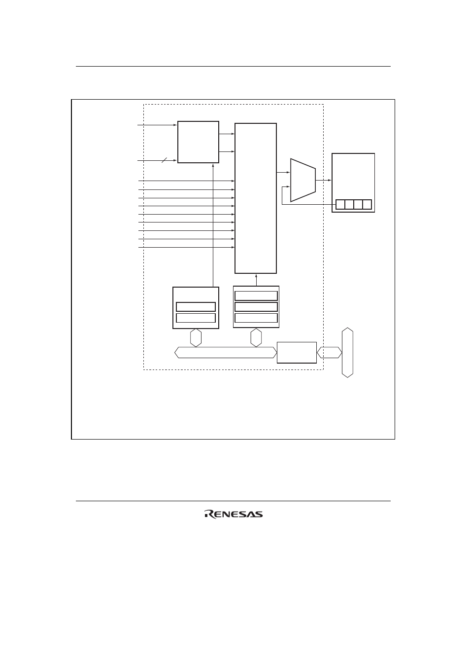
Figure 10.1 shows a block diagram of the intc, Figure 10.1 block diagram of intc – Renesas SH7641 User Manual
Page 270
Section 10 Interrupt Controller (INTC)
Rev. 4.00 Sep. 14, 2005 Page 220 of 982
REJ09B0023-0400
Figure 10.1 shows a block diagram of the INTC.
DMAC
SCIF0 to 2
ADC
USB
CMT0 and CMT1
MTU0 to MTU4
WDT
H-UDI
IIC2
8
DMAC:
SCIF:
ADC:
USB:
CMT:
MTU:
WDT:
H-UDI:
DMA controller
Serial communication interfaces (with FIFO) 0 to 2
A/D converter
USB funciton module
Compare match timers 0 and 1
Multifuncton timer pulse units 0 to 4
Watchdog timer
User debugging interface
IIC2:
ICR:
IPR:
IMR:
IMCR:
IRR0:
SR:
I
2
C interface 2
Interrupt control register
Interrupt priority registers B to J
Interrupt mask registers 0 to 10
Interrupt mask clear registers 0 to 10
Interrupt request register 0
Status register
I/O
controller
Priority
identifier
Com-
parator
Interrupt
request
SR
CPU
Bus
interface
Inter
nal b
us
Interrupt contoroller
I3 I2 I1 I0
(Interrupt request)
(Interrupt request)
(Interrupt request)
(Interrupt request)
(Interrupt request)
(Interrupt request)
(Interrupt request)
(Interrupt request)
(Interrupt request)
ICR
IRR0
[Legend]
IRQ7 to IRQ0
NMI
IPR
IMR
IMCR
Figure 10.1 Block Diagram of INTC