Renesas SH7641 User Manual
Page 516
Section 15 User Debugging Interface (H-UDI)
Rev. 4.00 Sep. 14, 2005 Page 466 of 982
REJ09B0023-0400
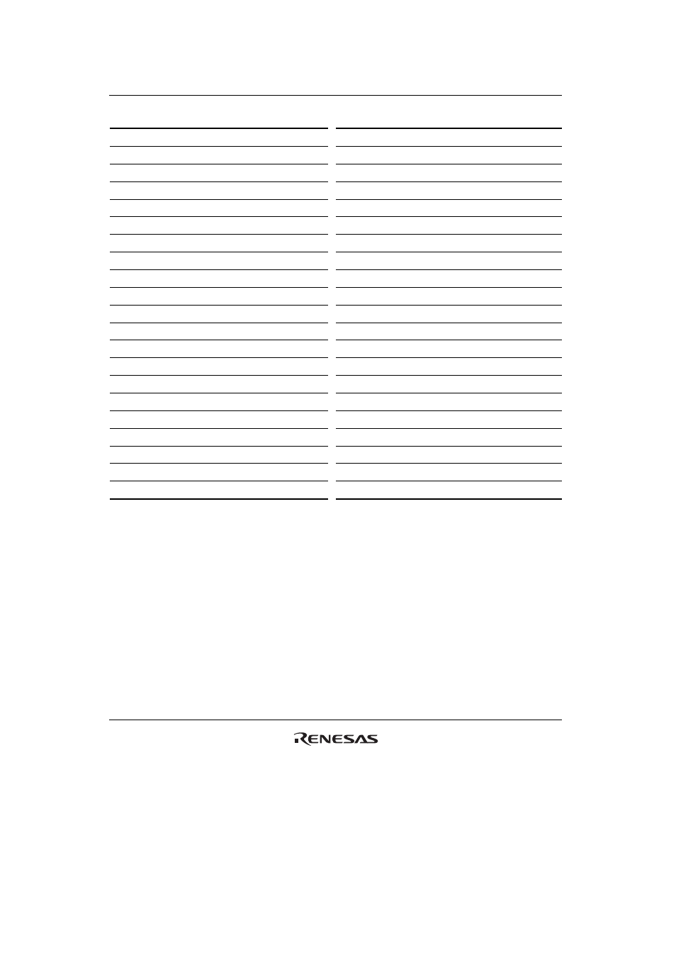
Bit Pin
Name
I/O
Bit Pin
Name
I/O
40 D20/PTD4
Control
19 A11
Control
39 D19/PTD3
Control
18 A10
Control
38 D18/PTD2
Control
17 A9
Control
37 D17/PTD1
Control
16 A8
Control
36 D16/PTD0
Control
15 A7
Control
35 RD/
WR Control
14
A6
Control
34
WE0/DQMLL Control
13
A5
Control
33
WE1/DQMLU Control
12
A4
Control
32
CASU/PTA5 Control
11
A3
Control
31
WE3/DQMUU/AH Control
10
A2
Control
30
RASU/PTA7 Control
9
A1
Control
29
WE2/DQMUL Control
8
A0/PTA0
Control
28 CKE/PTA1
Control
7 D15
Control
27
CASL/PTA4 Control
6
D14
Control
26
RASL/PTA6 Control
5
D13
Control
25 A17
Control
4 D12
Control
24 A16
Control
3 D11
Control
23 A15
Control
2 D10
Control
22 A14
Control
1 D9
Control
21 A13
Control
0 D8
Control
20 A12
Control
to
TDO
Notes: 1. Control is an active-high signal.
2. When Control is driven high, the corresponding pin is driven by the value of OUT.
3.
*VccQ is not the power supply for the LSI, but is still necessary for operation of the user
functions. Accordingly, pull this pin up in the way described in the specifications. These
pins must be pulled-up based on the specifications.