Renesas SH7641 User Manual
Page 409

Section 12 Bus State Controller (BSC)
Rev. 4.00 Sep. 14, 2005 Page 359 of 982
REJ09B0023-0400
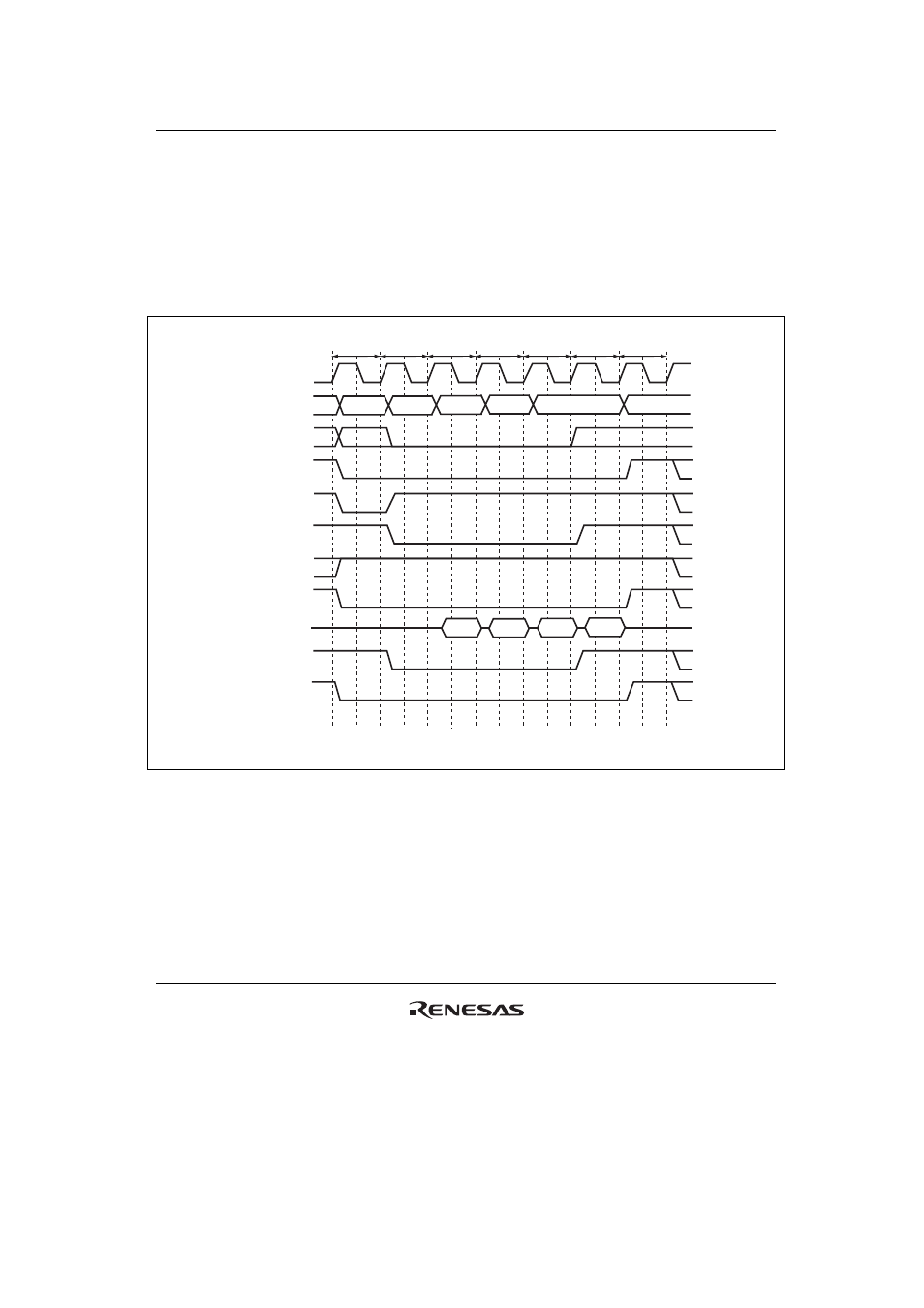
When bank active mode is set, if only accesses to the respective banks in the area 3 space are
considered, as long as accesses to the same row address continue, the operation starts with the
cycle in figure 12.23 or 12.26, followed by repetition of the cycle in figure 12.24 or 12.27. An
access to a different area during this time has no effect. If there is an access to a different row
address in the bank active state, after this is detected the bus cycle in figure 12.24 or 12.27 is
executed instead of that in figure 12.25 or 12.28. In bank active mode, too, all banks become
inactive after a refresh cycle or after the bus is released as the result of bus arbitration.
Tc4
Tr
Tc2
Tc3
Tc1
Td4
Td2
Td3
Td1
Tde
CKIO
A25 to A0
CSn
RD/
WR
RASL, RASU
DQMxx
D31 to D0
BS
DACKn*
2
A12/A11*
1
CASL, CASU
Notes: 1. Address pin to be connected to pin A10 of SDRAM.
2. The waveform for
DACKn is when active low is specified.
Figure 12.23 Burst Read Timing (Bank Active, Different Bank, CAS Latency 1)
