Renesas SH7641 User Manual
Page 80

Section 2 CPU
Rev. 4.00 Sep. 14, 2005 Page 30 of 982
REJ09B0023-0400
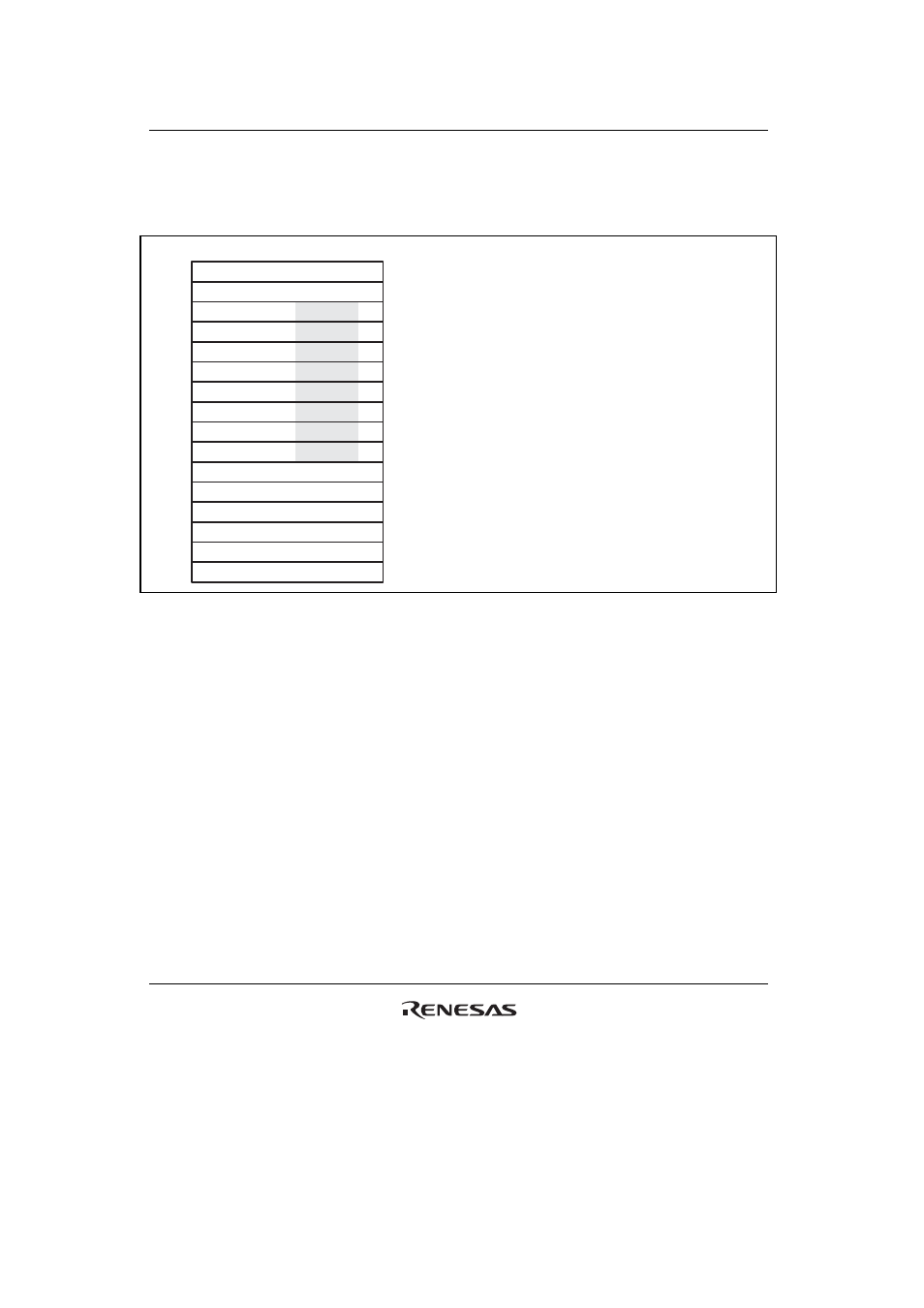
On the other hand, registers R2 to R9 are also used for DSP data address calculation when DSP
extension is enabled (see figure 2.4). Other symbols that represent the purpose of the registers in
DSP type instructions is shown in [ ].
31
R0
R1
R2 [As]
R3 [As]
R4 [As, Ax]
R5 [As, Ax]
R6 [Ay]
R7 [Ay]
R8 [Ix, Is]
R9 [Iy]
R10
R11
R12
R13
R14
R15
0
General Registers (DSP mode enabled)
X or Y data transfer operation
R4, 5 [Ax]: Address register set for X data memory.
R8 [x]:
Index register for address register set Ax.
R6, 7 [Ay]: Address register set for Y data memory.
R9 [Iy]:
Index register for address register set Ay.
Single data transfer operation
R2 to 5 [As]: Address register set for memory.
R8 [Is]:
Index register for address register set As.
Figure 2.4 General Registers (DSP Mode)
DSP type instructions can access X and Y data memory simultaneously. To specify addresses for
X and Y data memory, two address pointer sets are provided. These are:
R8[Ix], R4,5[Ax] for X memory access, and R9[Iy], R6,7[Ay] for Y memory access.
The symbols R2 to R9 are used by the assembler, but users can use other register names (aliases)
that indicate the purpose of the register in the DSP instruction. The coding in assembler is as
follows.
Ix:
.REG (R8)
The name Ix is the alias for R8. Other aliases are as follows.
Ax0: .REG (R4)
Ax1: .REG (R5)
Ix:
.REG
(R8)
Ay0: .REG (R6)
