Renesas SH7641 User Manual
Page 665

Section 18 Multi-Function Timer Pulse Unit (MTU)
Rev. 4.00 Sep. 14, 2005 Page 615 of 982
REJ09B0023-0400
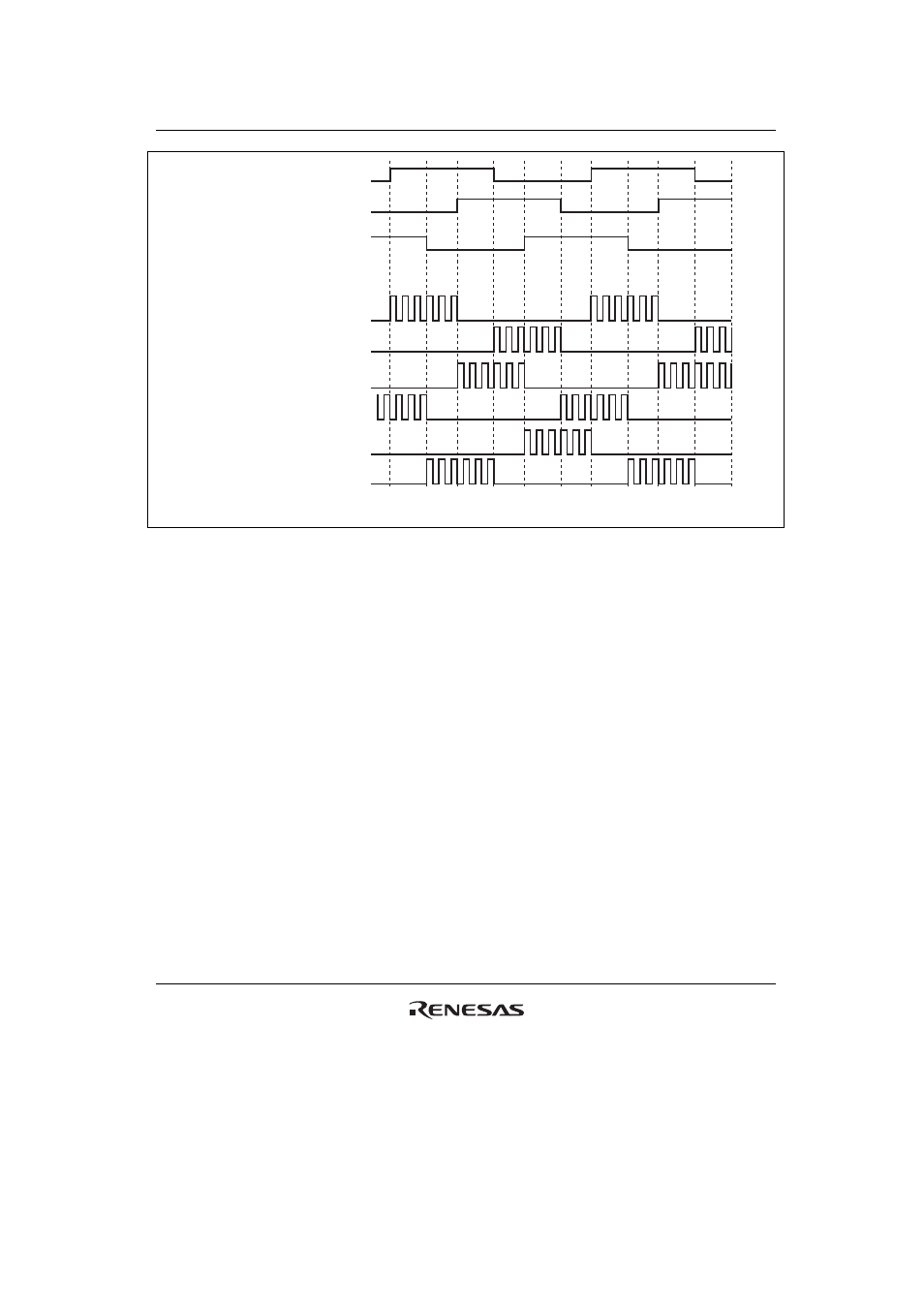
TGCR
UF bit
VF bit
WF bit
TIOC3B pin
TIOC3D pin
TIOC4A pin
TIOC4C pin
TIOC4B pin
TIOC4D pin
6-phase output
When BCD = 1, N = 1, P = 1, FB = 1, output active level = high
Figure 18.53 Example of Output Phase Switching by Means of UF, VF, WF Bit Settings (2)
A/D Conversion Start Request Setting: In complementary PWM mode, an A/D conversion start
request can be set using a TGRA_3 compare-match or a compare-match on a channel other than
channels 3 and 4.
When start requests using a TGRA_3 compare-match are set, A/D conversion can be started at the
center of the PWM pulse.
A/D conversion start requests can be set by setting the TTGE bit to 1 in the timer interrupt enable
register (TIER).
Complementary PWM Mode Output Protection Function
Complementary PWM mode output has the following protection functions.
Register and Counter Miswrite Prevention Function: With the exception of the buffer
registers, which can be rewritten at any time, access by the CPU can be enabled or disabled for the
mode registers, control registers, compare registers, and counters used in complementary PWM
mode by means of bit 0 (MTURWE) in PEMTURWER of the port E (port E MTU R/W enable
register).
