Renesas SH7641 User Manual
Page 670

Section 18 Multi-Function Timer Pulse Unit (MTU)
Rev. 4.00 Sep. 14, 2005 Page 620 of 982
REJ09B0023-0400
P
φ
External
clock
TCNT input
clock
TCNT
Falling edge
Falling edge
Rising edge
N-1
N
N+1
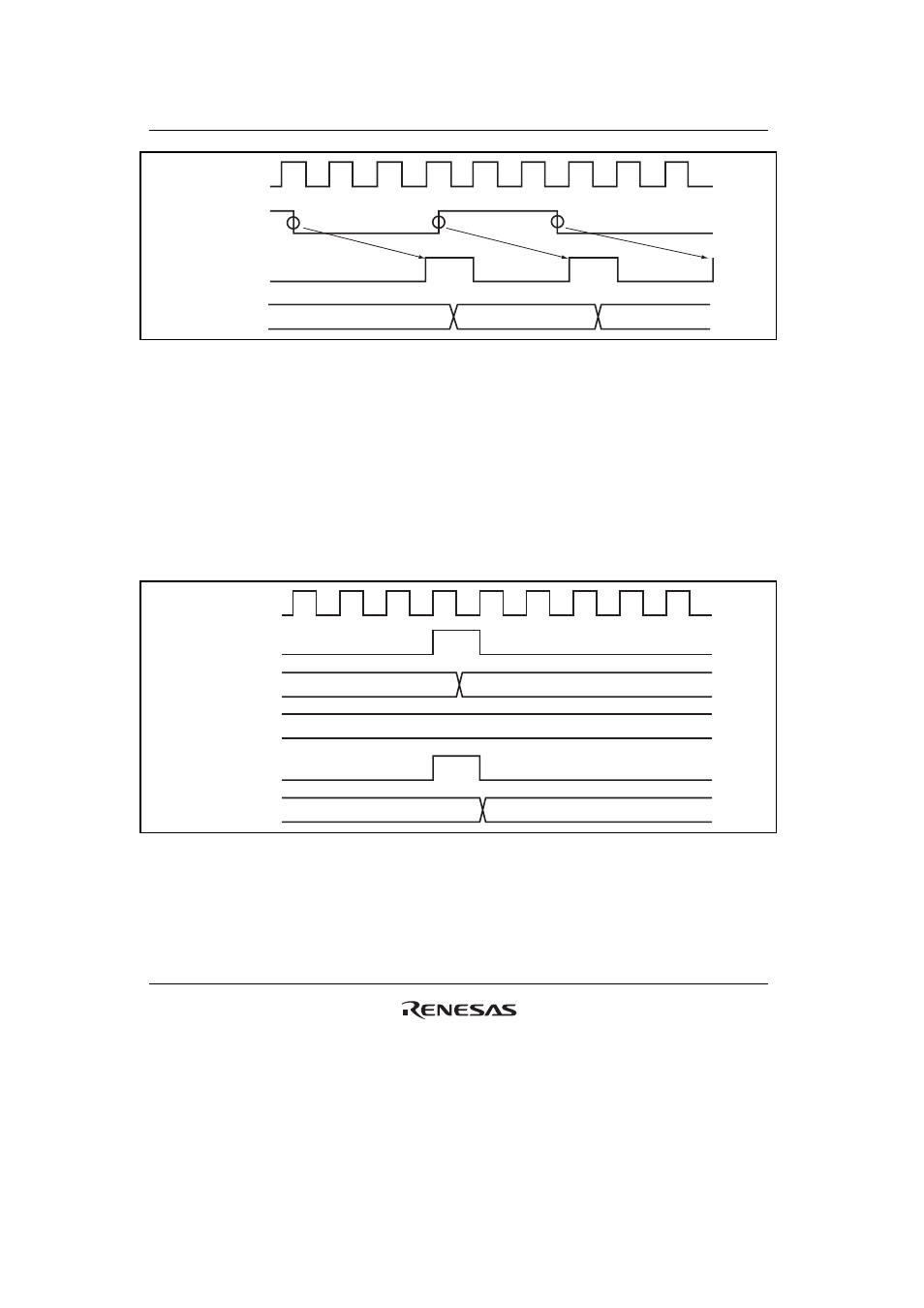
Figure 18.56 Count Timing in External Clock Operation (Phase Counting Mode)
Output Compare Output Timing: A compare match signal is generated in the final state in
which TCNT and TGR match (the point at which the count value matched by TCNT is updated).
When a compare match signal is generated, the output value set in TIOR is output at the output
compare output pin (TIOC pin). After a match between TCNT and TGR, the compare match
signal is not generated until the TCNT input clock is generated.
Figure 18.57 shows output compare output timing (normal mode and PWM mode) and
figure 18.58 shows output compare output timing (complementary PWM mode and reset
synchronous PWM mode).
TGR
TCNT
TCNT input
clock
N
N
N+1
Compare
match signal
TIOC pin
P
φ
Figure 18.57 Output Compare Output Timing (Normal Mode/PWM Mode)
