3 dma transfer overview, 4 dma controller module programming model – Motorola ColdFire MCF5281 User Manual
Page 300
DMA Controller Module
16-4
Freescale Semiconductor
16.3
DMA Transfer Overview
The DMA module can transfer data faster than the ColdFire core. The term “direct memory access” refers
to a fast method of moving data within system memory (including memory and peripheral devices) with
minimal processor intervention, greatly improving overall system performance. The DMA module
consists of four independent, functionally equivalent channels, so references to DMA in this chapter apply
to any of the channels. It is not possible to implicitly address all four channels at once.
The processor generates DMA requests internally by setting DCR[START]; the UART modules and DMA
timers can generate a DMA request by asserting internal DREQ signals. The processor can program bus
bandwidth for each channel. The channels support cycle-steal and continuous transfer modes; see
Section 16.5.1, “Transfer Requests (Cycle-Steal and Continuous Modes)
.”
The DMA controller supports dual-address transfers. The DMA channels support up to 32 data bits.
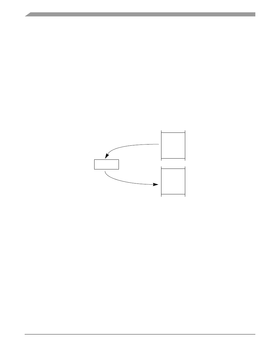
•
Dual-address transfers—A dual-address transfer consists of a read followed by a write and is
initiated by an internal request using the START bit or by asserting DREQ. Two types of transfer
can occur: a read from a source device or a write to a destination device. See
for more
information.
Figure 16-3. Dual-Address Transfer
Any operation involving the DMA module follows the same three steps:
1. Channel initialization—Channel registers are loaded with control information, address pointers,
and a byte-transfer count.
2. Data transfer—The DMA accepts requests for operand transfers and provides addressing and bus
control for the transfers.
3. Channel termination—Occurs after the operation is finished, either successfully or due to an error.
The channel indicates the operation status in the channel’s DSR, described in
“DMA Status Registers (DSR0–DSR3)
.”
16.4
DMA Controller Module Programming Model
This section describes each internal register and its bit assignment. Note that modifying DMA control
registers during a DMA transfer can result in undefined operation.
shows the mapping of DMA
controller registers. Note the differences for the byte count registers depending on the value of
MPARK[BCR24BIT]. See
Section 8.5.3, “Bus Master Park Register (MPARK)
” for further information.
DMA
DMA
Memory/
Peripheral
Memory/
Peripheral
Control and Data
Control and Data
MCF5282 and MCF5216 ColdFire Microcontroller User’s Manual, Rev. 3