Motorola ColdFire MCF5281 User Manual
Page 156
System Control Module (SCM)
8-4
Freescale Semiconductor
The physical base address programmed in both copies of the RAMBAR is typically the same value;
however, they can be programmed to different values. By definition, the base address must be a
0-modulo-size value.
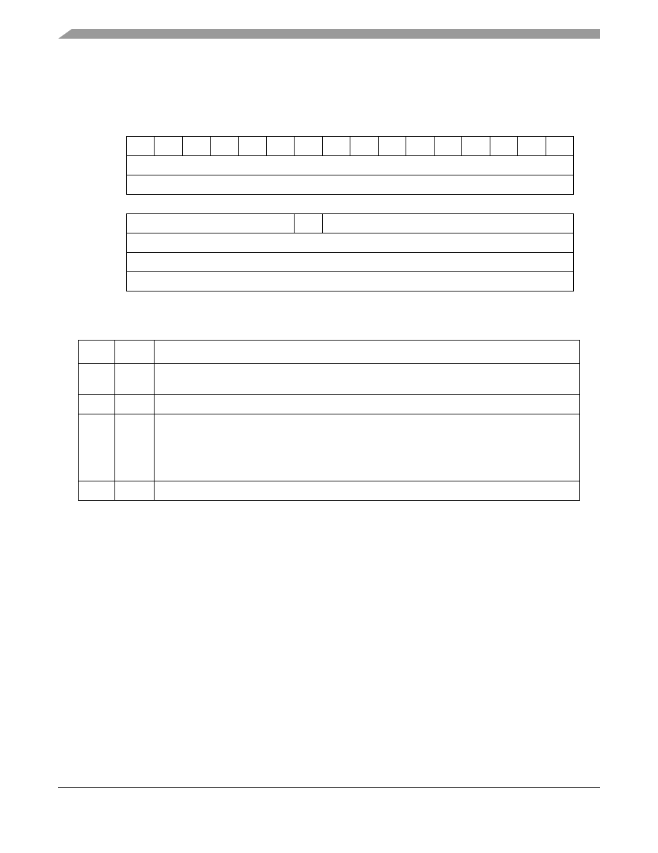
The SRAM modules are configured through the RAMBAR shown in
•
RAMBAR specifies the base address of the SRAM.
•
All undefined bits are reserved. These bits are ignored during writes to the RAMBAR and return
zeros when read.
•
The back door enable bit, RAMBAR[BDE], is cleared at reset, disabling the module access to the
SRAM.
NOTE
The RAMBAR default value of 0x0000_0000 is invalid. The RAMBAR
located in the processor’s CPU space must be initialized with the valid bit
set before the CPU (or modules) can access the on-chip SRAM (see
For details on the processor's view of the local SRAM memories, see
Section 5.3.1, “SRAM Base Address
31
30
29
28
27
26
25
24
23
22
21
20
19
18
17
16
Field BA31 BA30 BA29 BA28 BA27 BA26 BA25 BA24 BA23 BA22 BA21 BA20 BA19 BA18 BA17 BA16
Reset
0000_0000_0000_0000
R/W
R/W
15
10
9
8
0
Field
—
BDE
—
Reset
0000_0000_0000_0000
R/W
R/W
Address
IPSBAR + 0x008
Figure 8-2. Memory Base Address Register (RAMBAR)
Table 8-3. RAMBAR Field Description
Bits
Name
Description
31–16
BA
Base address. Defines the memory module's base address on a 64-Kbyte boundary corresponding
to the physical array location within the 4 Gbyte address space supported by ColdFire.
15–10
—
Reserved, should be cleared.
9
BDE
Back door enable. Qualifies the module accesses to the memory.
0 Disables module accesses to the memory.
1 Enables module accesses to the memory.
NOTE: The SPV bit in the CPU’s RAMBAR must also be set to allow dual port access to the SRAM.
For more information, see
Section 5.3.1, “SRAM Base Address Register (RAMBAR)
.”
8–0
—
Reserved, should be cleared.
MCF5282 and MCF5216 ColdFire Microcontroller User’s Manual, Rev. 3