3 conversion timing schemes, 3 conversion timing schemes -58 – Motorola ColdFire MCF5281 User Manual
Page 596
Queued Analog-to-Digital Converter (QADC)
28-58
Freescale Semiconductor
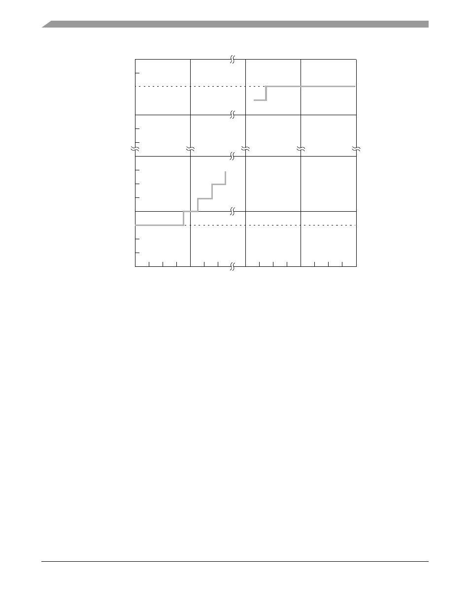
Figure 28-45. Errors Resulting from Clipping
28.9.3
Conversion Timing Schemes
This section contains some conversion timing examples.
conversions where it is assumed that:
•
Q1 begins with CCW0 and ends with CCW3.
•
CCW0 has pause bit set.
•
CCW1 does not have pause bit set.
•
External trigger rising edge for Q1
•
CCW4 = BQ2 and Q2 is disabled.
•
Q1 RES shows relative result register updates.
Recall that when QS = 0, both queues are disabled; when QS = 8, queue 1 is active and queue 2 is idle;
and when QS = 4; queue 1 is paused and queue 2 is disabled.
0
.020
5.100
5.110
1
2
3
4
5
6
7
8
3FA
3FB
3FC
3FD
3FE
3FF
.010
.030
5.120
5.130
10-b
it Re
sult (H
e
x
ade
cimal)
Inputs in Volts (V
RH
= 5.120 V, V
RL
= 0 V)
MCF5282 and MCF5216 ColdFire Microcontroller User’s Manual, Rev. 3