Figure 26-8, Figure 26-9, Figure 26-10 – Motorola ColdFire MCF5281 User Manual
Page 512
General Purpose I/O Module
26-12
Freescale Semiconductor
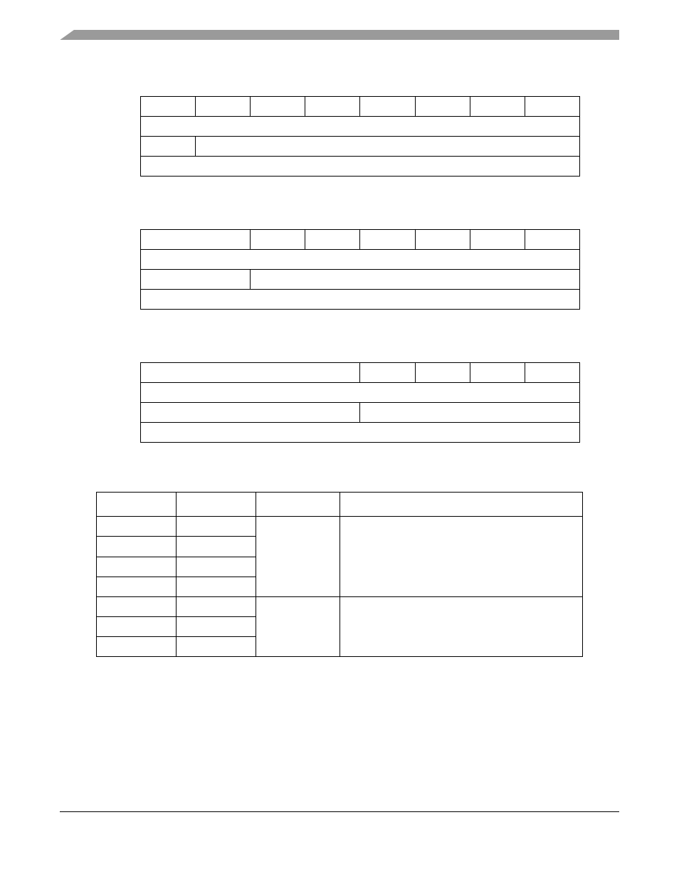
7
6
0
Field
—
DDRn6
DDRn5
DDRn4
DDRn3
DDRn2
DDRn1
DDRn0
Reset
0000_0000
R/W:
R
R/W
Address
IPSBAR + 0x10_0021(DDRQS)
Figure 26-8. Port Data Direction Register (7-bit)
7
6
5
4
3
2
1
0
Field
—
DDRn5
DDRn4
DDRn3
DDRn2
DDRn1
DDRn0
Reset
0000_0000
R/W:
R
R/W
Address
IPSBAR + 0x10_0020 (DDRAS), 0x10_0022 (DDRSD)
Figure 26-9. Port Data Direction Registers (6-bit)
7
4
3
2
1
0
Field
—
DDRn3
DDRn2
DDRn1
DDRn0
Reset
0000_0000
R/W:
R
R/W
Address
IPSBAR + 0x10_0023 (DDRTC), 0x10_0024 (DDRTD), 0x10_0025 (DDRUA)
Figure 26-10. Port Data Direction Registers (4-bit)
Table 26-4. DDRn (8-bit, 6-bit, and 4-bit) Field Descriptions
Register
Bits
Name
Description
8-bit
7–0
DDRnx
Port n data direction bits.
1 Port n pin configured as an output
0 Port n pin configured as an input
7-bit
6–0
6-bit
5–0
4-bit
3–0
7-bit
7
—
Reserved, should be cleared.
6-bit
7–6
4-bit
7–4
MCF5282 and MCF5216 ColdFire Microcontroller User’s Manual, Rev. 3