2 thermal characteristics, 2 thermal characteristics -2, Dition – Motorola ColdFire MCF5281 User Manual
Page 686: Current, Table 33-2 lists thermal resistance values, Never exceeds v

Electrical Characteristics
33-2
Freescale Semiconductor
33.2
Thermal Characteristics
lists thermal resistance values.
2
This device contains circuitry protecting against damage due to high static voltage or electrical
fields; however, it is advised that normal precautions be taken to avoid application of any
voltages higher than maximum-rated voltages to this high-impedance circuit. Reliability of
operation is enhanced if unused inputs are tied to an appropriate logic voltage level (e.g., either
V
SS
or V
DD
).
3
Not applicable for MCF5280.
4
Input must be current limited to the value specified. To determine the value of the required
current-limiting resistor, calculate resistance values for positive and negative clamp voltages,
then use the larger of the two values. 6.0V voltage excludes XTAL and EXTAL pads.
5
All functional non-supply pins are internally clamped to V
SS
and V
DD
.
6
Power supply must maintain regulation within operating V
DD
range during instantaneous and
operating maximum current conditions. If positive injection current (V
in
> V
DD
) is greater than
I
DD
, the injection current may flow out of V
DD
and could result in external power supply going
out of regulation. Insure external V
DD
load will shunt current greater than maximum injection
current. This will be the greatest risk when the MCU is not consuming power (ex; no
clock).Power supply must maintain regulation within operating V
DD
range during instantaneous
and operating maximum current conditions.
7
All ESD testing methodology is in conformity with CDF-AEC-Q100 Stress Test Qualification for
Automotive Grade Integrated Circuits.
NOTE
It is crucial during power-up that V
DD
never
exceeds V
DDH
by more than
≈0.3 V. There are
diode devices between the two voltage domains,
and violating this rule can lead to a latch-up
condition.
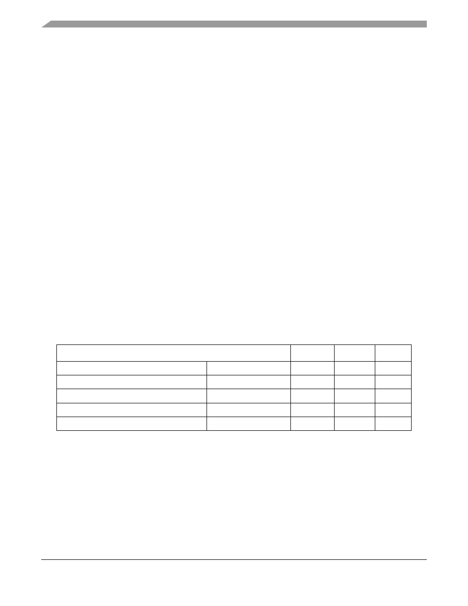
Table 33-2. Thermal Characteristics
Characteristic
Symbol
Value
Unit
Junction to ambient, natural convection
Four layer board (2s2p)
θ
JMA
26
1,2
1
θ
JMA
and
Ψ
jt
parameters are simulated in accordance with EIA/JESD Standard 51-2 for natural convection.
Freescale recommends the use of
θ
JA
and power dissipation specifications in the system design to prevent device
junction temperatures from exceeding the rated specification. System designers should be aware that device
junction temperatures can be significantly influenced by board layout and surrounding devices. Conformance to the
device junction temperature specification can be verified by physical measurement in the customer’s system using
the
Ψ
jt
parameter, the device power dissipation, and the method described in EIA/JESD Standard 51-2.
2
Per JEDEC JESD51-6 with the board horizontal.
°C/W
Junction to ambient (@200 ft/min)
Four layer board (2s2p)
θ
JMA
23
1,2
°C/W
Junction to board
θ
JB
15
3
3
Thermal resistance between the die and the printed circuit board per JEDEC JESD51-8. Board temperature is
measured on the top surface of the board near the package.
°C/W
Junction to case
θ
JC
10
4
4
Thermal resistance between the die and the case top surface as measured by the cold plate method (MIL SPEC-883
Method 1012.1).
°C/W
Junction to top of package
Natural convection
Ψ
jt
°C/W
MCF5282 and MCF5216 ColdFire Microcontroller User’s Manual, Rev. 3
