1 read a/d register (rareg/rdreg), 2 write a/d register (wareg/wdreg) – Motorola ColdFire MCF5281 User Manual
Page 641
Debug Support
Freescale Semiconductor
30-23
NOTE
The BDM status bit (S) is 0 for normally completed commands; S = 1 for
illegal commands, not-ready responses, and transfers with bus-errors.
Section 30.5.2, “BDM Serial Interface
,” describes the receive packet
format.
Freescale reserves unassigned command opcodes for future expansion. Unused command formats in any
revision level perform a
NOP
and return an illegal command response.
30.5.3.3.1
Read A/D Register (
RAREG
/
RDREG
)
Read the selected address or data register and return the 32-bit result. A bus error response is returned if
the CPU core is not halted.
Command/Result Formats:
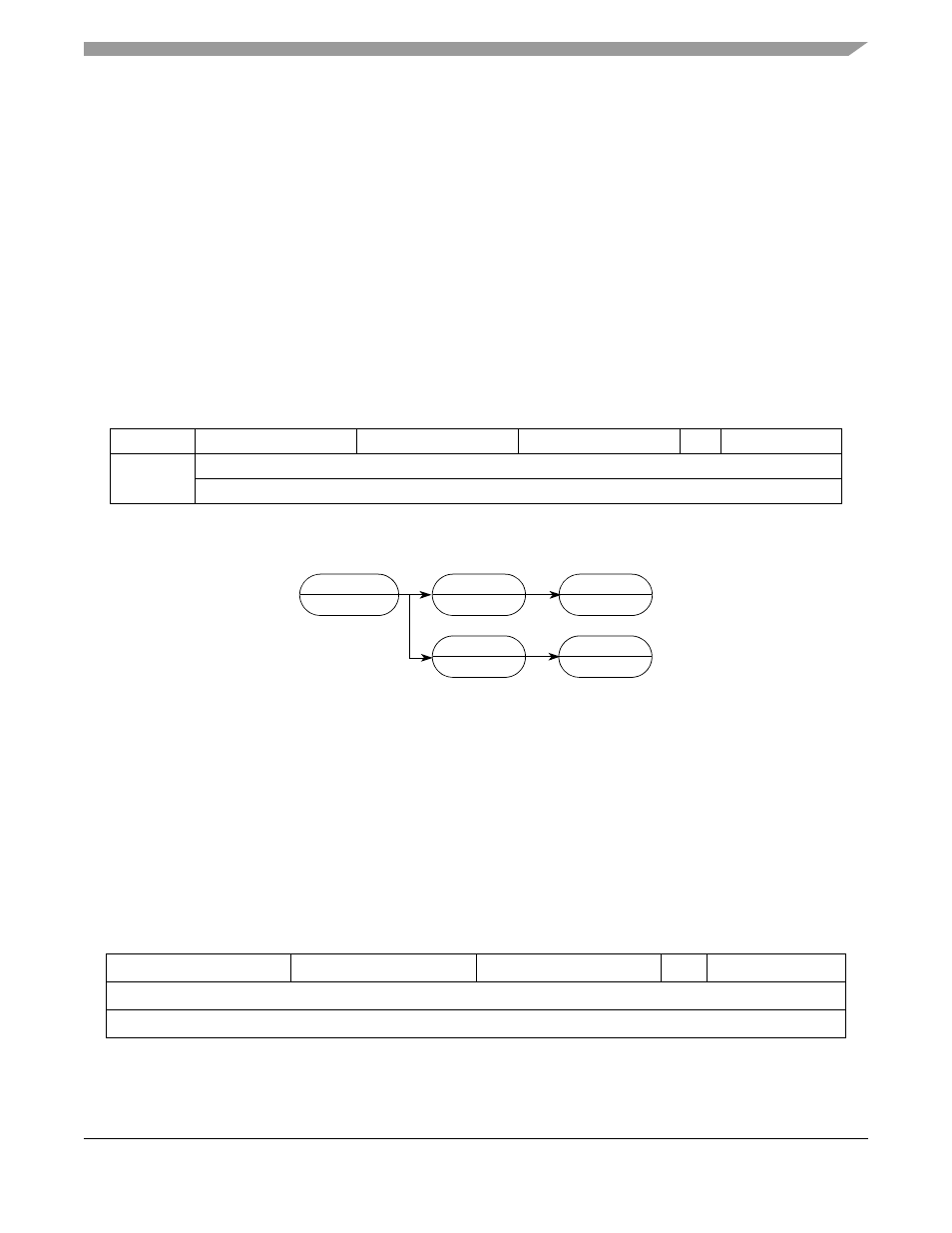
Command Sequence:
Figure 30-18.
RAREG
/
RDREG
Command Sequence
Operand Data:
None
Result Data:
The contents of the selected register are returned as a longword value,
most-significant word first.
30.5.3.3.2
Write A/D Register (
WAREG
/
WDREG
)
The operand longword data is written to the specified address or data register. A write alters all 32 register
bits. A bus error response is returned if the CPU core is not halted.
Command Format:
15
12
11
8
7
4
3
2
0
Command
0x2
0x1
0x8
A/D
Register
Result
D[31:16]
D[15:0]
Figure 30-17.
RAREG
/
RDREG
Command Format
15
12
11
8
7
4
3
2
0
0x2
0x0
0x8
A/D
Register
D[31:16]
D[15:0]
Figure 30-19.
WAREG
/
WDREG
Command Format
RAREG/RDREG
???
NEXT CMD
LS RESULT
NEXT CMD
’NOT READY’
XXX
BERR
XXX
MS RESULT
MCF5282 and MCF5216 ColdFire Microcontroller User’s Manual, Rev. 3